
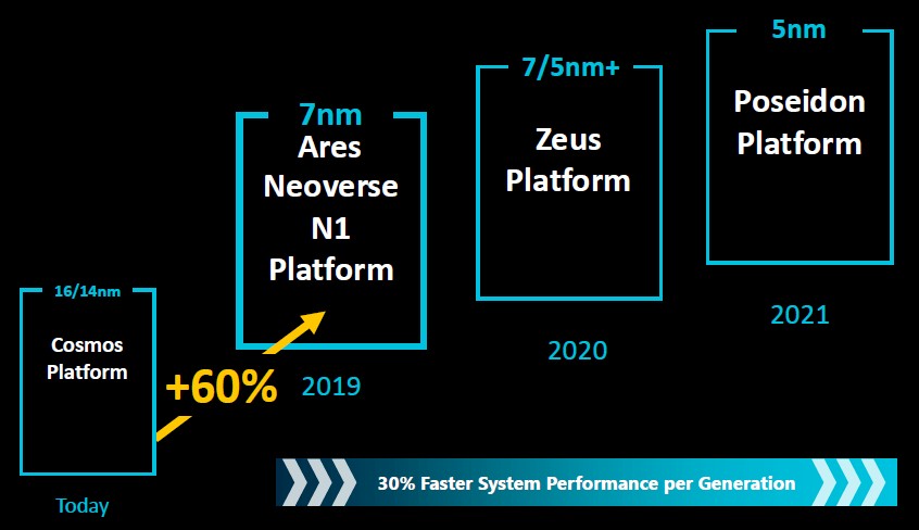
When Arm Holdings, the division of the Softbank conglomerate that designs and licenses the core component of the processor architecture that bears its name, launched its Neoverse revamping of the Arm architecture for the datacenter and the edge last October, the company put the architecture on a strict annual cadence and promised to deliver 30 percent performance increases at the system level with each generation.
This is an ambitious set of performance and process node goals. And straight out of the chute this year, with the “Ares” Neoverse designs, which will henceforth be known as the N1, Arm is doing one better and guaranteeing a baseline of more than double that performance, and is showing gains of much more than this on many workloads that are being tested on prototype chips and simulators. It is not so much that Arm low-balled the performance gains it thought it could get with the Ares chips so much as a lot of different factors in hardware and compilers are coming together at the same time to make a boost that is bigger than Arm had planned when it started the Neoverse project, which seeks to deliver processor designs tuned specifically for the datacenter core and edge, over five years ago.
When we suggested to Mike Filippo, who is an Arm Fellow and lead architect for engineering, at a recent Tech Day event in San Jose for selected chipheads, that the engineers could now coast like crazy, he laughed and said, “You might think so, but unfortunately on the engineering side, just because we overshoot here doesn’t mean we can undershoot there. We just make our jobs harder.”
All joking aside, we probably should not get used to Arm beating its own performance goals so dramatically. While there is always a chance that performance can be pushed higher, each process node is harder to work with and it is always tough to predict how other technologies within a system will continue to evolve. Even 30 percent performance – again, at the system level – every year means that performance is 2.2X higher than the baseline three years into the future. This is better than the Intel Xeon architecture has been delivering in recent years, and a little bit faster than the pace that IBM has delivered in its Power7 through Power9 generations from 2010 through 2018.
Frankly, it was time for Arm to get a lot more creative with its server core designs, with the Cortex-A72 and Cortex-A75 cores not having enough oomph and therefore compelling the company’s server partners to invest in creating custom 64-bit core designs. This has had the effect of slowing down the delivery of server designs as Arm advances the architecture, and hopefully going forward more Arm licensees that are already in the server space or who aspire to be can take these Neoverse designs, add in the memory controllers, PHYs, and PCI-Express controllers that Arm does not supply and very quickly get tapeouts to their fab of choice and get chips into the field. (It is really down to Taiwan Semiconductor Manufacturing Corp at this point, with some possibilities perhaps with Samsung Electronics, maybe someday United Microelectronic Corp of China, and – if hell freezes right over solid like quartz – maybe Intel. GlobalFoundries is out of the game of pushing processes and is hanging back at the 14/16 nanometer node.)
The Ares designs are tuned for the 7 nanometer node at TSMC; it is not clear just how much the HiSilicon division of Huawei Technology relied on the Ares design to create its Kunpeng 920 processor, which it revealed back in early January and which will ship later this year. But the Kunpeng 920, despite what HiSilicon says about designing its own Armv8 core, looks an awful lot like the 64-core Ares reference chip, with eight DDR4 memory controllers and PCI-Express 4.0 peripheral controllers, that Arm unveiled at that Tech Day event. Hmmmm….
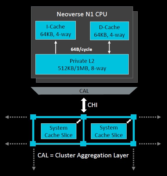
With the Neoverse designs, Arm is moving from the ring topology linking elements of the system on chip with the Cortex-A72 to a mesh topology that has higher bandwidth across the components and lower latency between them, on average, and it is this, perhaps more than anything, that is giving the Ares Neoverse N1 chip such a big performance boost compared to its “Cosmos” predecessor based on a modified Cortex-A72. Here is what the compute element of the Ares chip looks like:
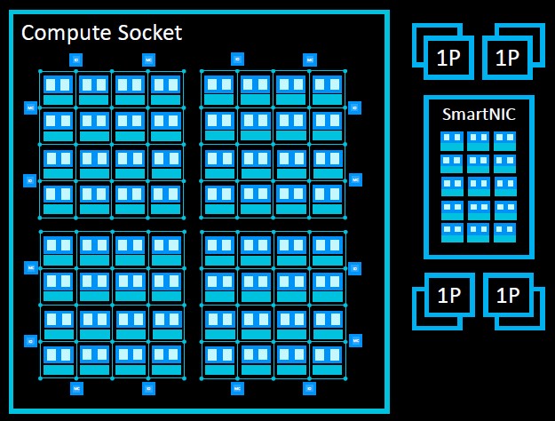
“This has been a five year labor of love, across many development sites, to create a new set of infrastructure products,” explains Filippo. “We came into the project concurrently optimizing for performance, power efficiency, and areal efficiency, and this is important. If we had gone after absolute peak single threaded performance, we would have been leaving throughput on the table. This is a fine balancing act. The power efficiency that we bring to bear is really there to enable us to have very high core count systems, at full frequency sustained all day long with any workload that you want to throw at it. The Ares will scale up – we will talk big numbers all day long – but it will also scale down. We have a processor that will scale up to high end datacenter systems all the way down to low power SmartNICs.”
The maximum clock speed of the cores on the Ares N1 chip as etched in the initial 7 nanometer processes from TSMC tops out at around 3.5 GHz, according to Filippo, with customers licensing the Neoverse N1 designs expected to push the clock speeds in the range of 2.6 GHz to 3.1 GHz typically to fit into certain thermal design points for server, storage, and networking devices.
The Ares core has 64 KB of L1 instruction cache and 64 KB of data cache, and the neat thing with this design, which is not something that is technically required by the Armv8.2 specification, is that the instruction caches are coherent. Depending on the make and model, the Ares design offers 512 KB or 1 MB of private L2 cache per core, and the core complex has a special high bandwidth, low latency pipe called Direct Connect that links the cores to the new mesh interconnect that lashes together all of the cores and the other elements of the system on chip.
The Ares core has a new and deeper pipeline that can be reconfigured on the fly to have fewer stages when the clock frequencies are jacked up to the hilt and the lowest latency possible through the core is desired. Here is what it looks like:
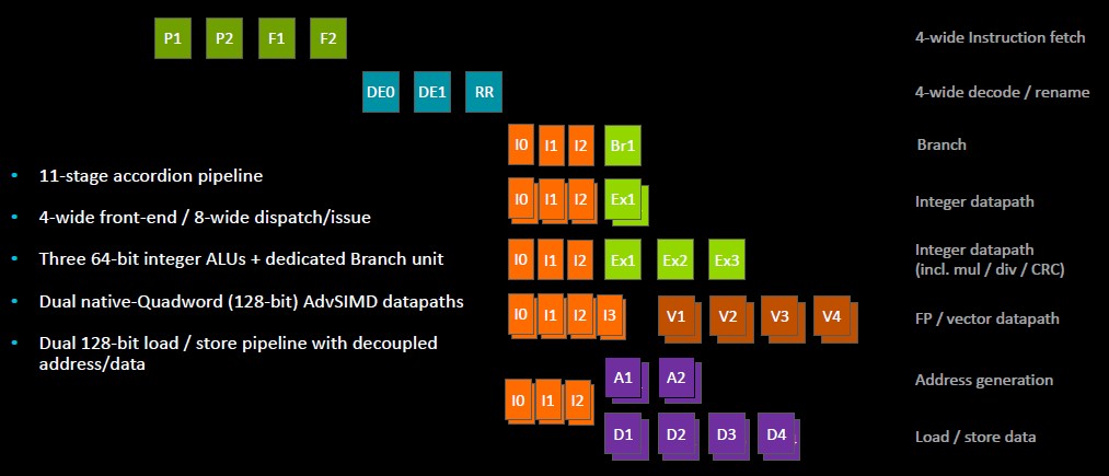
The N1 core pipeline has an 11-stage “accordion” pipeline that can scale back to 9 stages. The 11-stage pipeline has full access to the 1 MB shared L2 cache on the chip, which is spread around the mesh in segments matching to cores up to 128 MB for a device with 128 cores. When dropping back to the 9-stage pipeline, the L2 cache chunks gear back to 512 KB and that provides the lower latency that is required for having fewer stages running at a higher frequency. That L2 system level cache, what Arm calls SLC, runs full out on a 128-core device and delivers more than 1 TB/sec of aggregate bandwidth across those L2 cache segments hanging off the mesh.
There are separate and decoupled fetch pipes and branch pipes in the Ares core. The core has three 64-bit integer Arithmetic Logic Units (ALUs) plus a dedicated branch unit, and downstream from the integer units are two 128-bit AdvSIMD vector math units, which are twice as wide as the vector units in the Cortex-A72.
“We have effectively doubled the overall floating point bandwidth from the prior generation,” explains Filippo. “These are native quad-word, dual 128-bit units fed by separate issue queues and going into latency optimized execution pipelines. These latencies are two cycles for floating point add, three cycle for floating point multiply, and four cycle floating point multiply add. So we are pushing the latency on our AdvSIMD units pretty hard.”
The upshot of the Ares core is that it is designed to run flat out with all of its cores cranked and yet also be able to cope with the hefty, branch heavy virtual machine/hypervisor, database, and application serving workloads that are typical in the modern datacenter. It is interesting that the Ares architecture does not have L3 cache as its last level, but there is nothing stopping Arm licensees from adding this if they think it will add to the architecture. (We did not get the impression that Arm thinks L3 cache is useful, an opinion that more than a few chip designers share; others, notably Intel and IBM, disagree.)
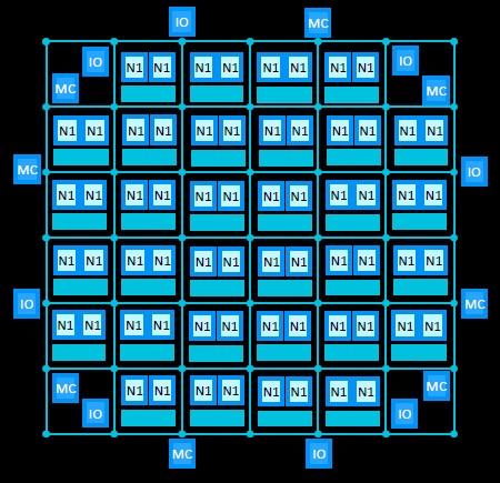
The DDR4 memory controllers and PCI-Express 4.0 peripheral controllers hang off the Ares interconnect mesh, just like the core complexes do. Here is what it looks like logically with a 64-core design:
This hypothetical chip shown above assumes a monolithic design, but that is not the only option. To lower the manufacturing costs of the overall socket, Ares licensees can decide to break the monolith into chiplets, like this:
In this case, the 64-core die is broken into four 16-core segments, and CCIX interconnects coming off the mesh are used to link the four chiplets into one logical processor. By the way, more CCIX links can also be added over the PCI-Express transport to create NUMA interconnects between sockets. (AMD’s Infinity Fabric on the Epyc X86 server processors similarly use a quad chiplet design and tweaked PCI-Express interconnects to create multi-chip modules for a socket and to link multiple sockets together.) Our guess is that the Ares architecture has enough PCI-Express bandwidth to handle some peripherals and maybe do four-socket NUMA boxes. This would cover the needs of the vast majority of the systems market.
The bandwidth of that mesh in the Ares design is considerably higher than the ring in the Cortex-A72 design. A monolithic 64-core test chip has a peak of 200 GB/sec of aggregate memory bandwidth per socket, according to Filippo, and running the STREAM Triad memory benchmark test, it is coming in at around 175 GB/sec. A 32-core Cortex-A72 reference design could deliver 64 GB/sec tops on STREAM Triad. On the LMBench microbenchmark test suite for C/C++ applications, that Cortex-A72 had an average latency of 110 nanoseconds; the 64-core Ares test chip came in at 83 nanoseconds. That’s a pretty big drop in latency as these things go – a 25 percent drop in latency is a big deal in any device – and nearly a factor of three higher bandwidth per socket.
The Ares core design, says Filippo, offers 30 percent better performance per watt than the Cortex-A72 if both were implemented in the same 7 nanometer process, and that is a pretty rare architectural re-engineering, indeed. The shrink from 16 nanometers to 7 nanometers allows for the core counts on a design to, in theory, be doubled with some clock uplift on top of that. That 64-core Ares test design will come in at around 105 watts for its thermal design point, with a single core delivering a SPECint_rate2006 of about 37 per core and 1,310 across 64 cores within that thermal envelope. (That is on the GCC8 compiler stack.) As for floating point performance, using the GCC7 compilers, that 64-core chip will do SPECfp_rate2006 of around 1,200, Arm estimates. (We will be drilling down into the expected performance of the Ares design separately, and the gains are quite large on various workloads compared to Cortex-A72 systems.)
The Ares designs are expected to scale up to 128 cores with 150 watts and possibly beyond as clock speeds are pushed, with smaller edge devices scaling down to 16 core to 64 core designs with between 35 watts and 105 watts of heat dissipation. Ares chips for network, storage, and security devices will scale between 8 cores and 32 cores with between 25 watts and 65 watts being burned.

Drilling Down Into The SiPearl European Arm Server Chip
The European Union has made it clear that it wants to be able to stand on its own two feet in the design of server processors, for both general purpose uses and for exascale-class supercomputers. It is a difficult task, and one that Silicon Pearl, a French startup founded by …

AMD Finally Breaks The 10 Percent Server Share Barrier
History doesn’t really repeat itself, but it surely does use a lot of synonyms and rhymes, and sometimes, if you listen very closely, you can catch it muttering to itself. It is with this in mind that we contemplate the recent data coming out of Mercury Research, which is the …

The Other Way To Bring Arm CPUs To Servers
There are at least two – and possibly more – paths to make Arm processors competitive with the Intel and now AMD X86 incumbent processors in the datacenter. The first path, and the one taken by most of the Arm collective to date, is to create a better CPU based …
Be the first to comment