
This is a complete soldering guide for installing NVMe SSD on the A1286 MacBook Pro 15-inch 2011/2012.
This guide is intended for enthusiasts with intermediate level of soldering skills and tools.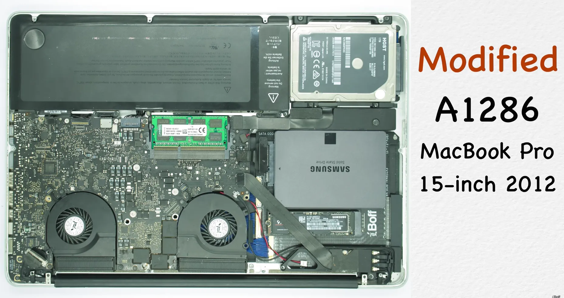
For those who have received the NevBolt-2 NVMe Kit: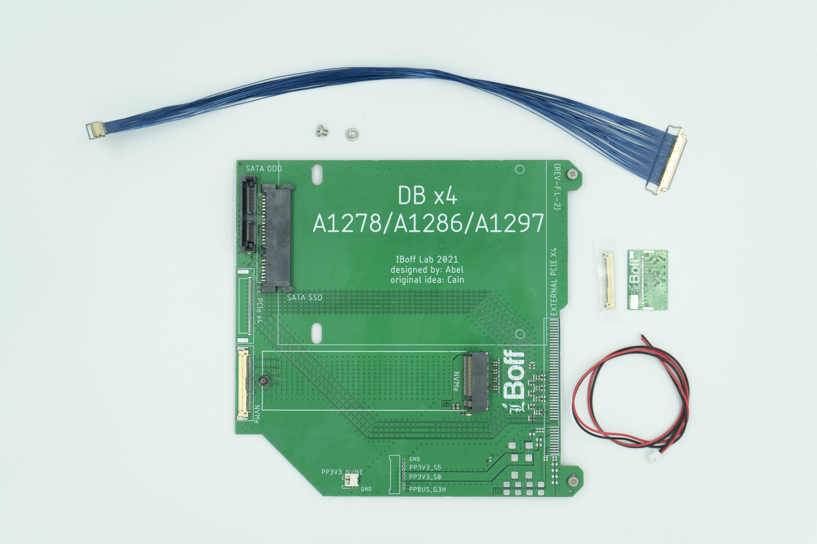
You should check the contents inside the package and it should have:
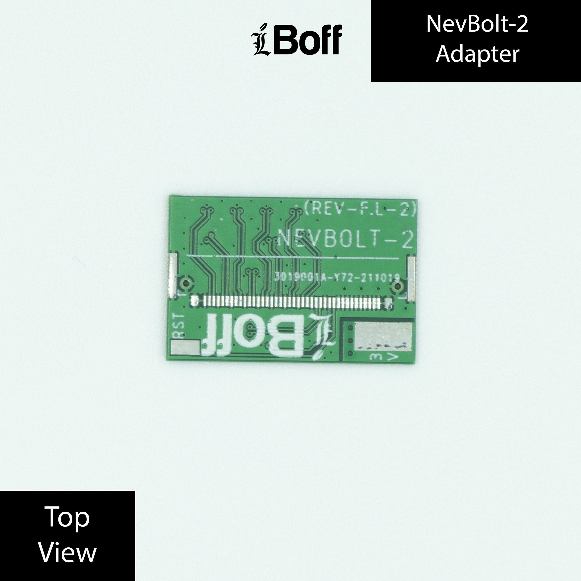
1 x NevBolt-2 adapter (for A1286) :
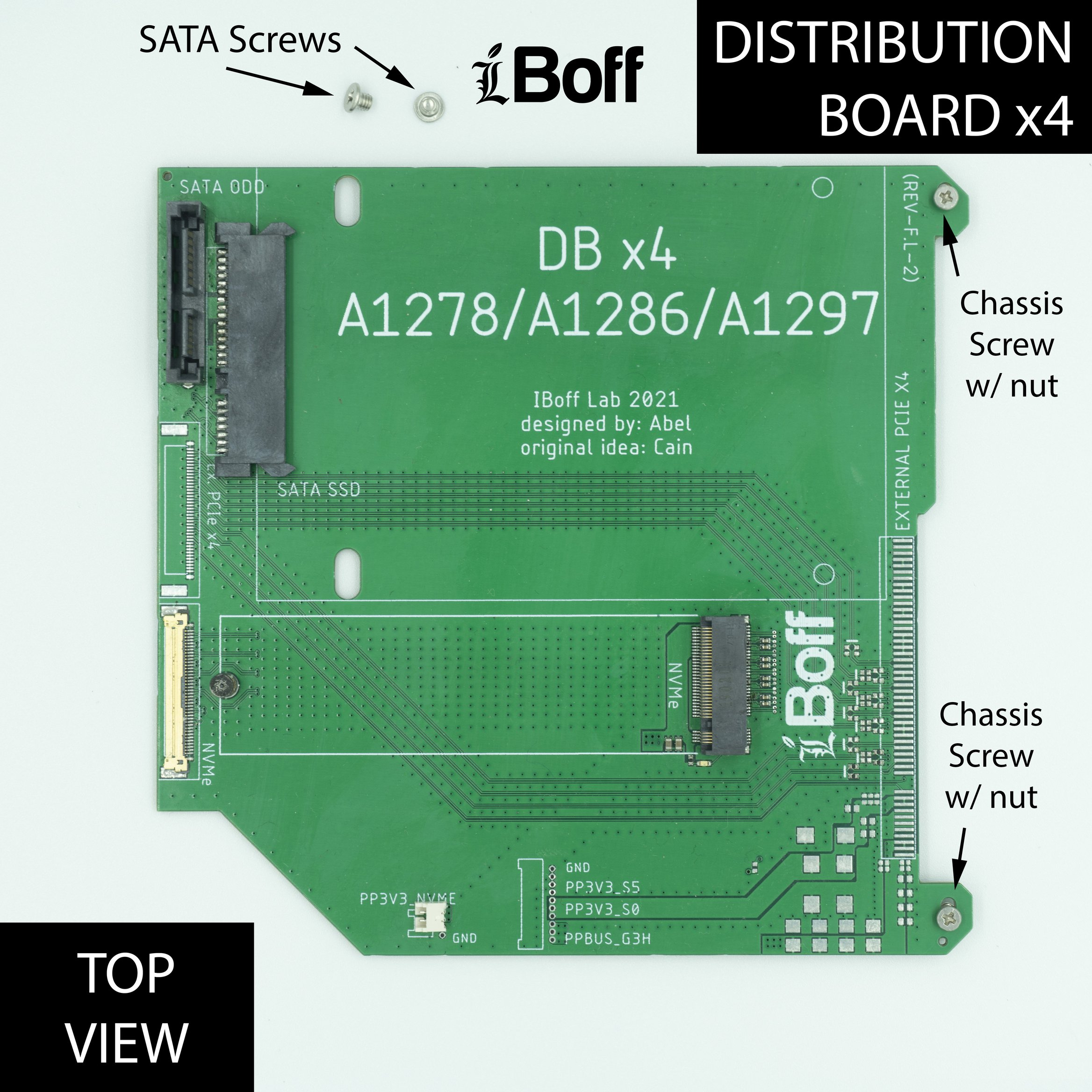
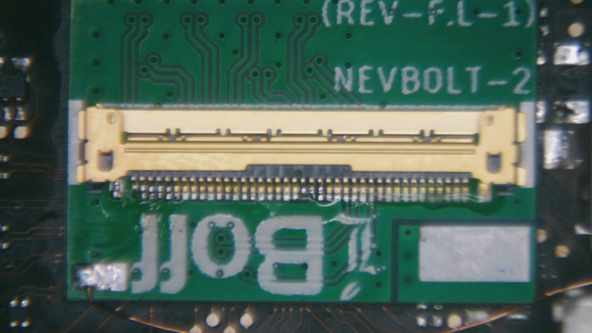
1x Distribution Board for A1286 that has an M.2 NVMe port :
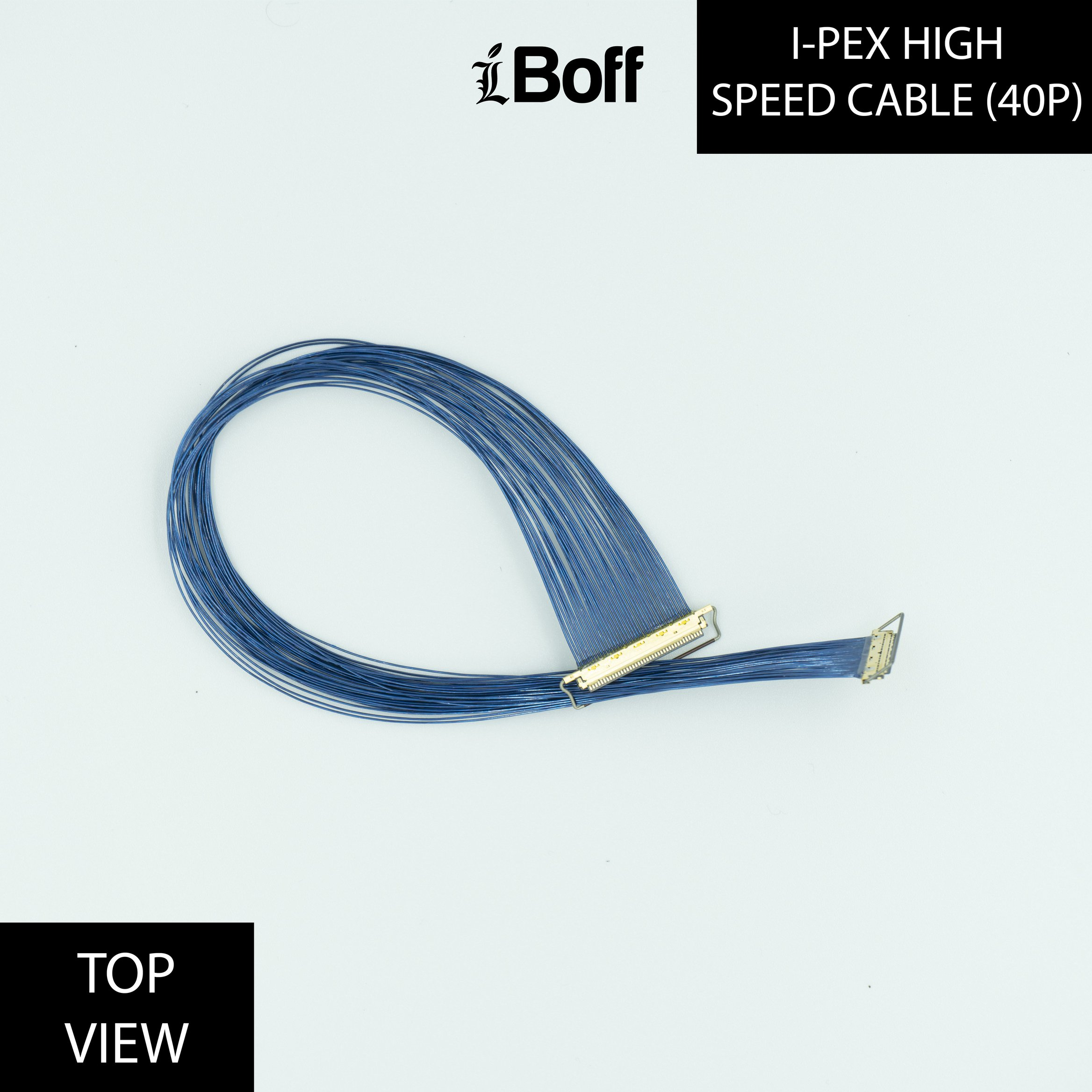
1x I-PEX high speed cable (blue colored) :
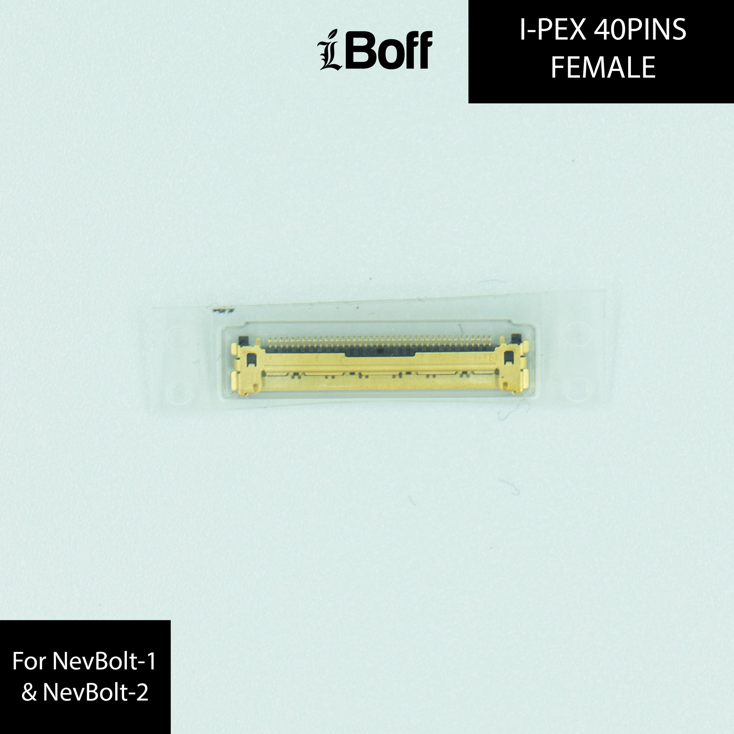
1x I-PEX 40 Pins connector :
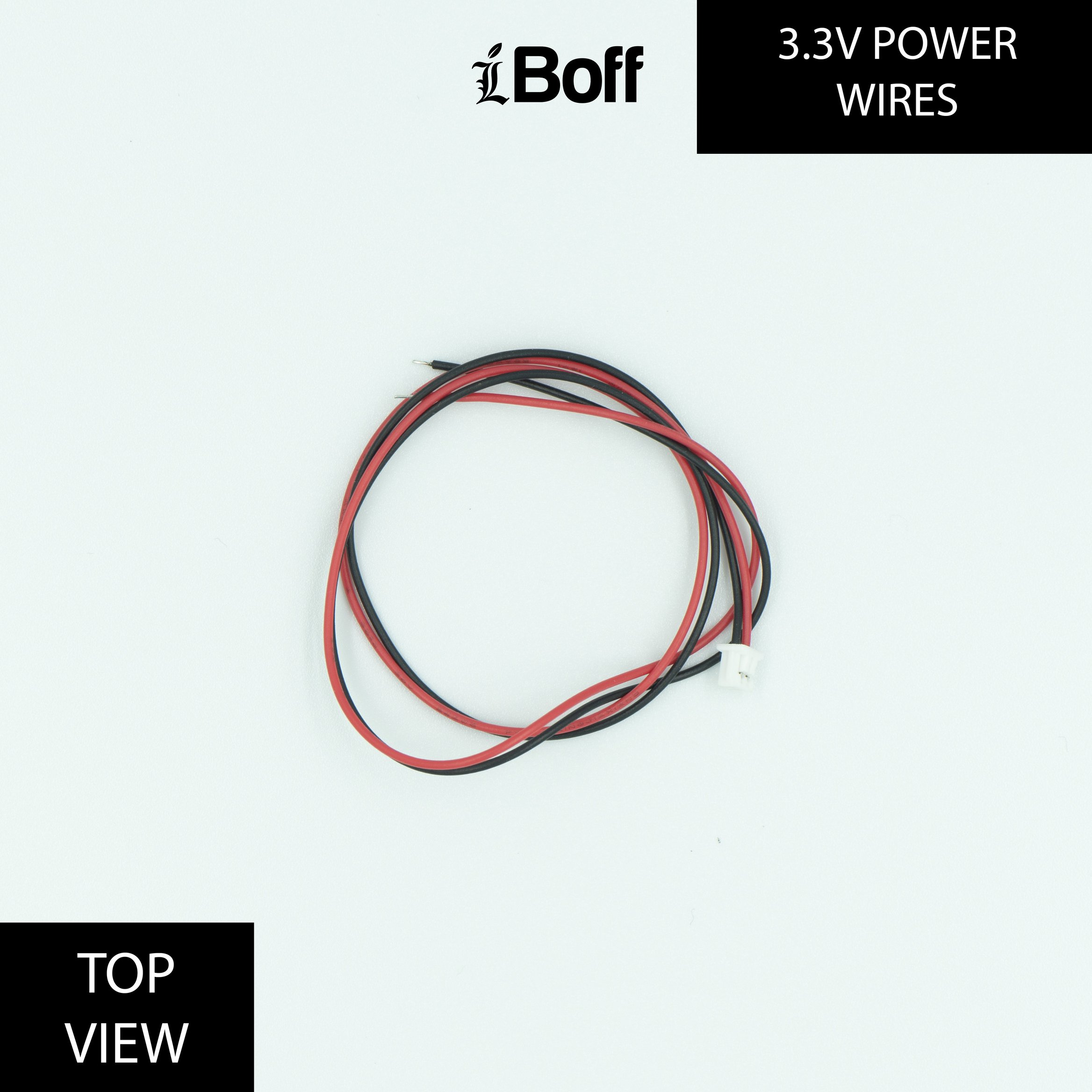
1x 3.3 Volt power wires (Red/Black) :
So the first step is you need to disassemble a good working A1286 MacBook Pro and take its logic board out of its chassis without damaging the related components. If you’re not sure how to do that, maybe you should not proceed any further.

Remove the DC-in jack and both of the RAM sticks, and all other heat sensitive components to avoid melting them. For the heatsink, we’re gonna leave it as it is for now to protect the CPU.
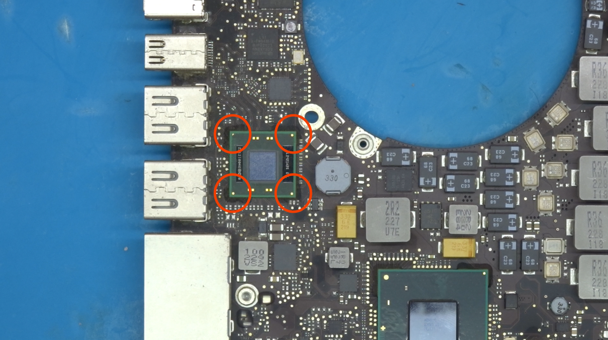
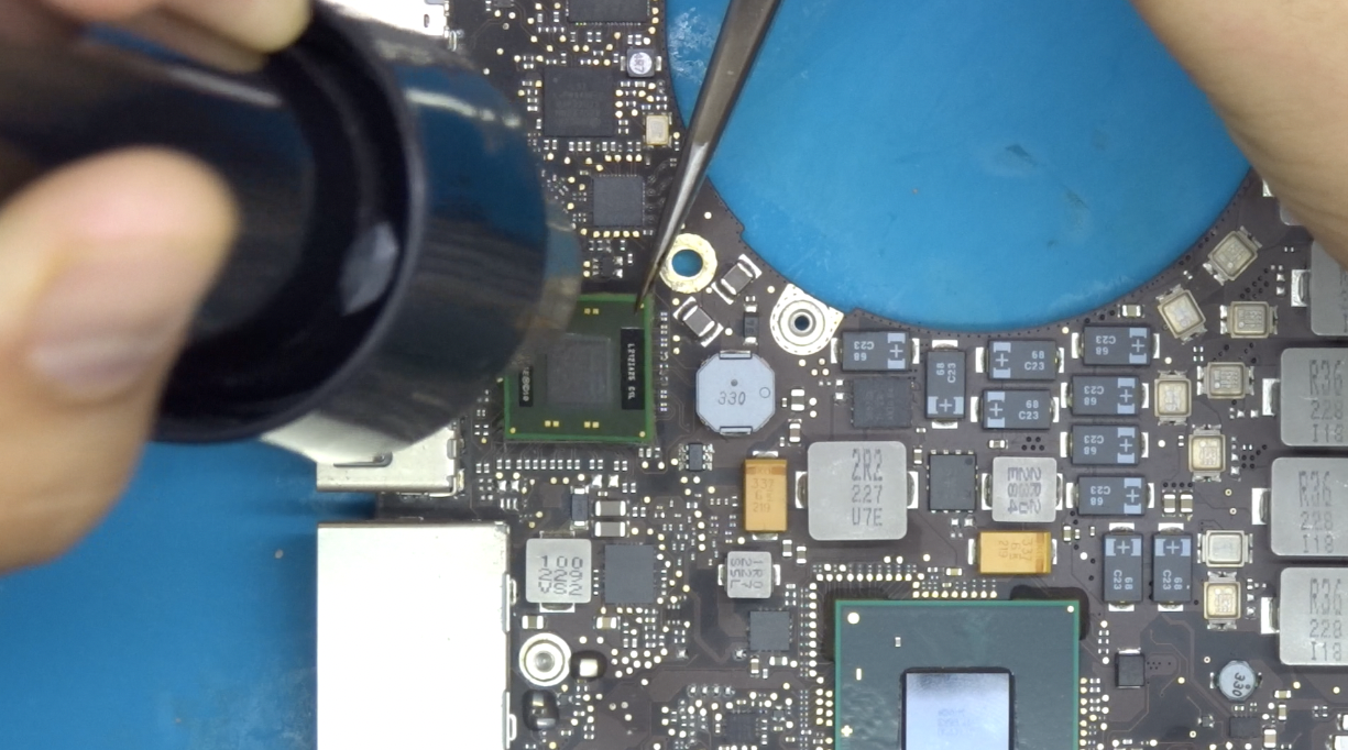
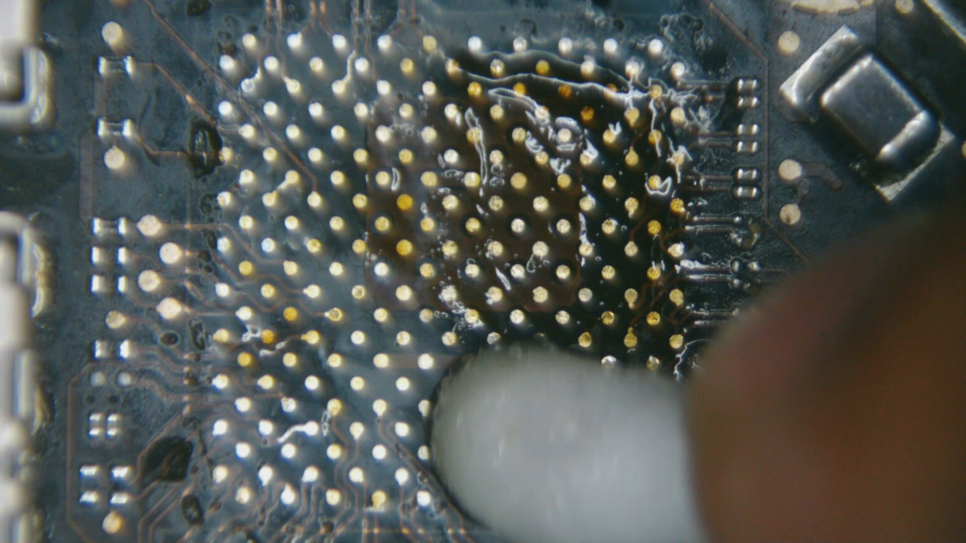
Next, you need to remove the silicone epoxy around the Thunderbolt 1 chip using the hot air gun.
 Usually we’ll use the highest temperature and air settings on the Quick hot air (857DW+), with the nozzle on, and the heat reaching the MLB is controlled by adjusting distance from the board. By blowing the hot air to the epoxy by maintaining 2-inch distance from the target, the surrounding epoxy should become soft so you can carefully remove them using a pair of tweezers.
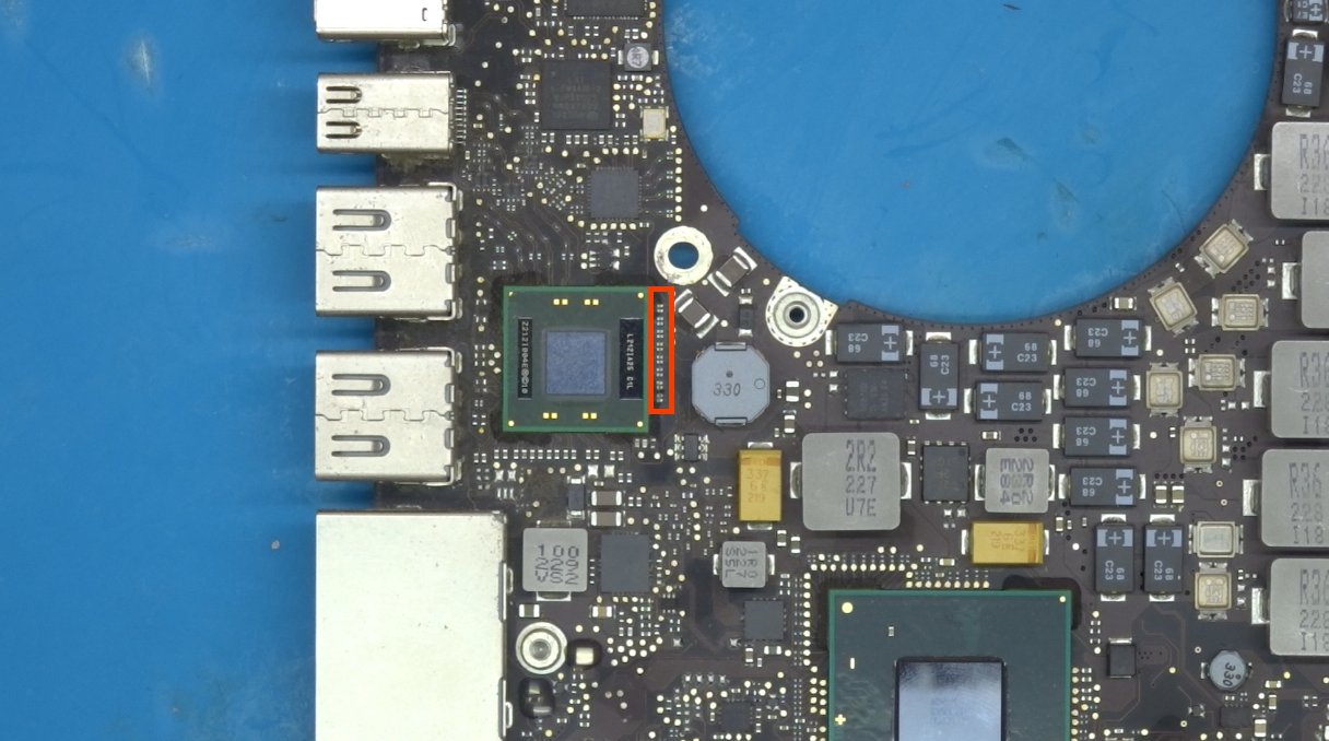
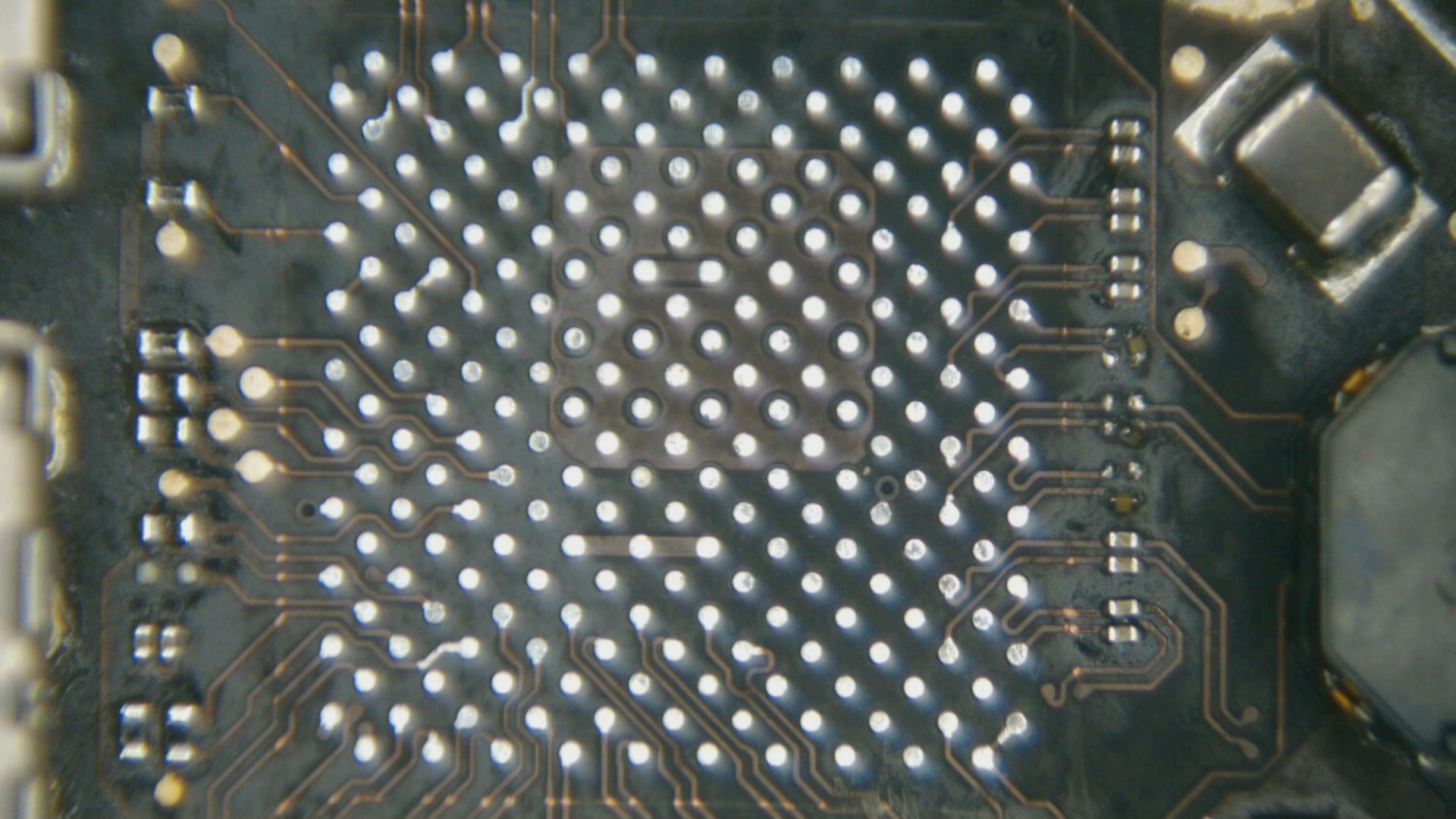
After the epoxy has been removed, LIGHTLY scratch the solder mask on the right side, upper side, left side, and finally lower side of the Thunderbolt 1 chip(represented as red rectangle).
 It is important to note that you should only scratch the solder mask layer at the TOP LAYER, not the COPPER LAYER beneath, or else the copper traces beneath the solder mask will deform and break. These lines will assist you for the NevBolt-2 positioning later on.
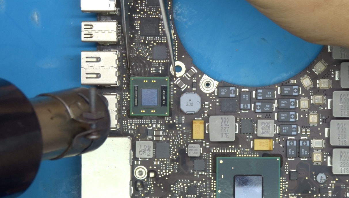
Take off the nozzle from the hot air gun to allow better heat distribution across the board to make the desoldering process easier. Before we are pointing the heat directly on the target(Thunderbolt chip), we need to preheat the local area first, as shown in the highlighted area.
Move the hot air gun in a circular motion targeting the local area, maintaining around 1-inch distance from the board as we’re giving time for the board layers to absorb heat and distribute the heat across the board evenly. 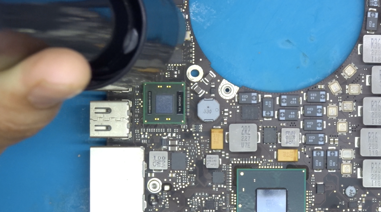
This preheating method will prevent thermal shock or thermal stress to the TBT chip, and also to prevent delamination of the board layers beneath that is useful in this project. 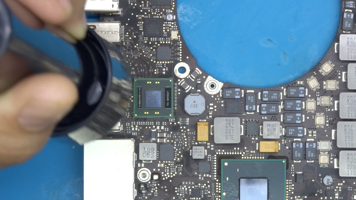 The concept is almost like removing the SMC chip, so actually this is not the only way to do it, but at least it works really great for us.

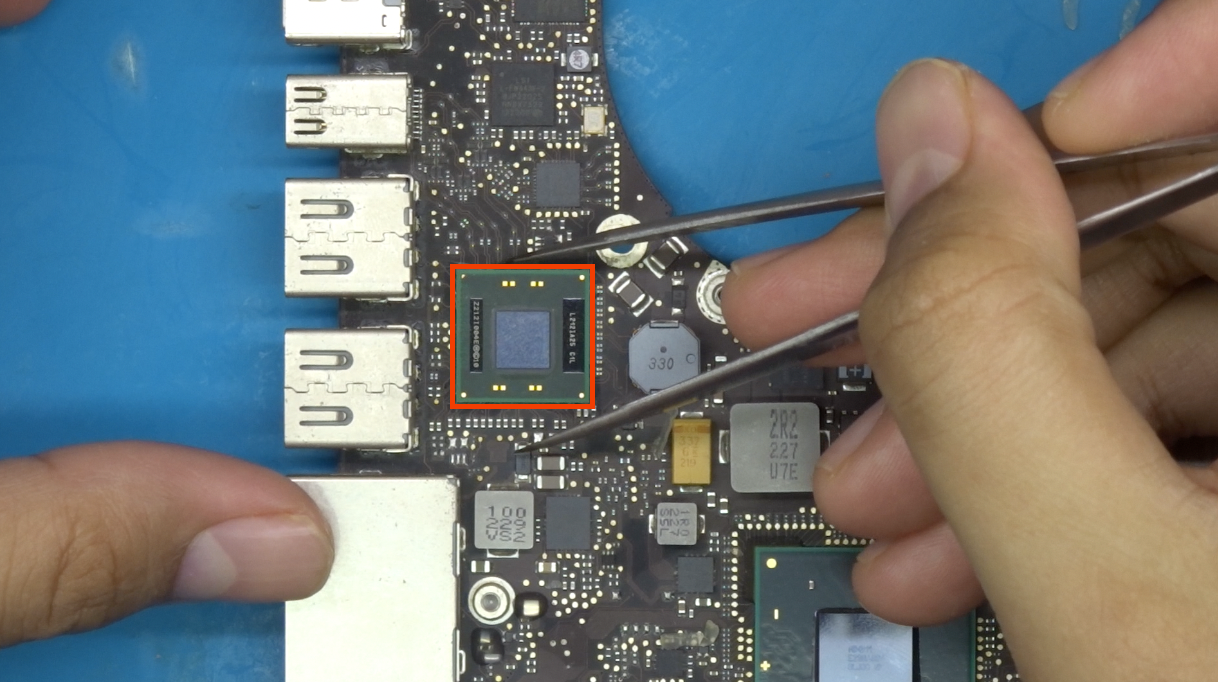
As you preheat the local area for around 1 minute, the board should already retain enough heat, so bring the hot air tip closer to the board, targeting the TBT chip. One of the ways to know if it is safe to take off the chip, is to poke the AC coupling capacitors at the side of the TBT chip.
These capacitors will need to be removed later, so it's perfectly fine if we mess with it now. 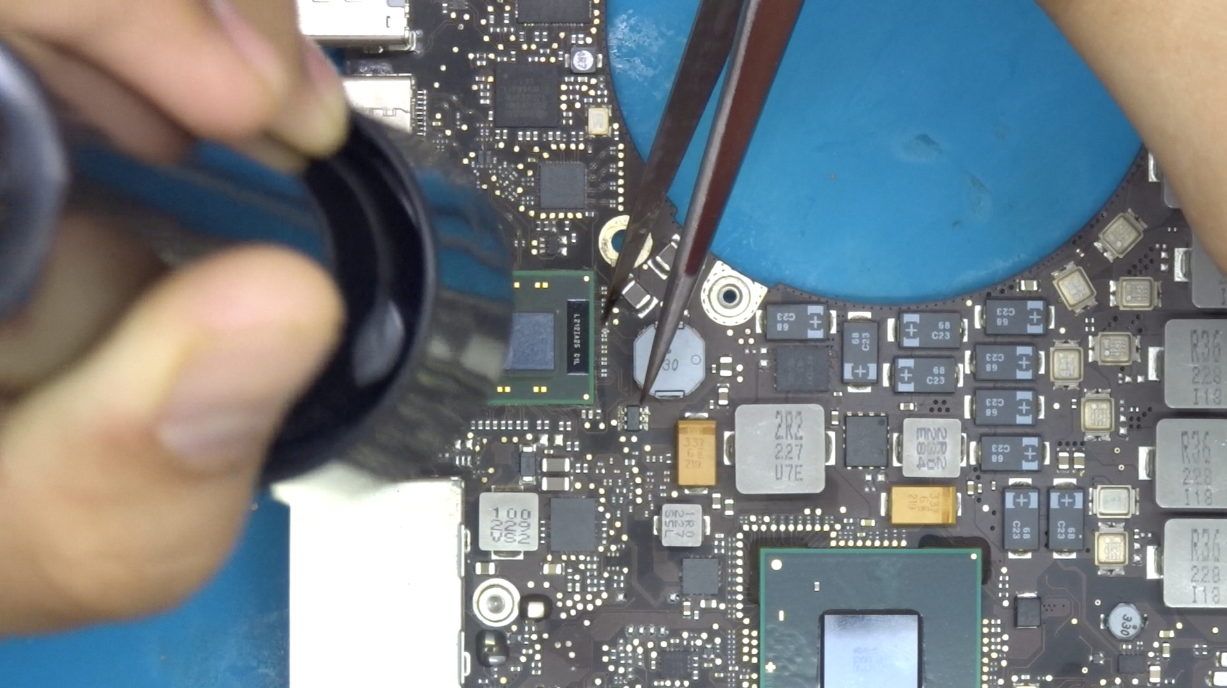 If you can move the caps, it means the lead free solder on that area already reaches liquidus temperature, so you can slowly try to lift the TBT chip using the tweezers.
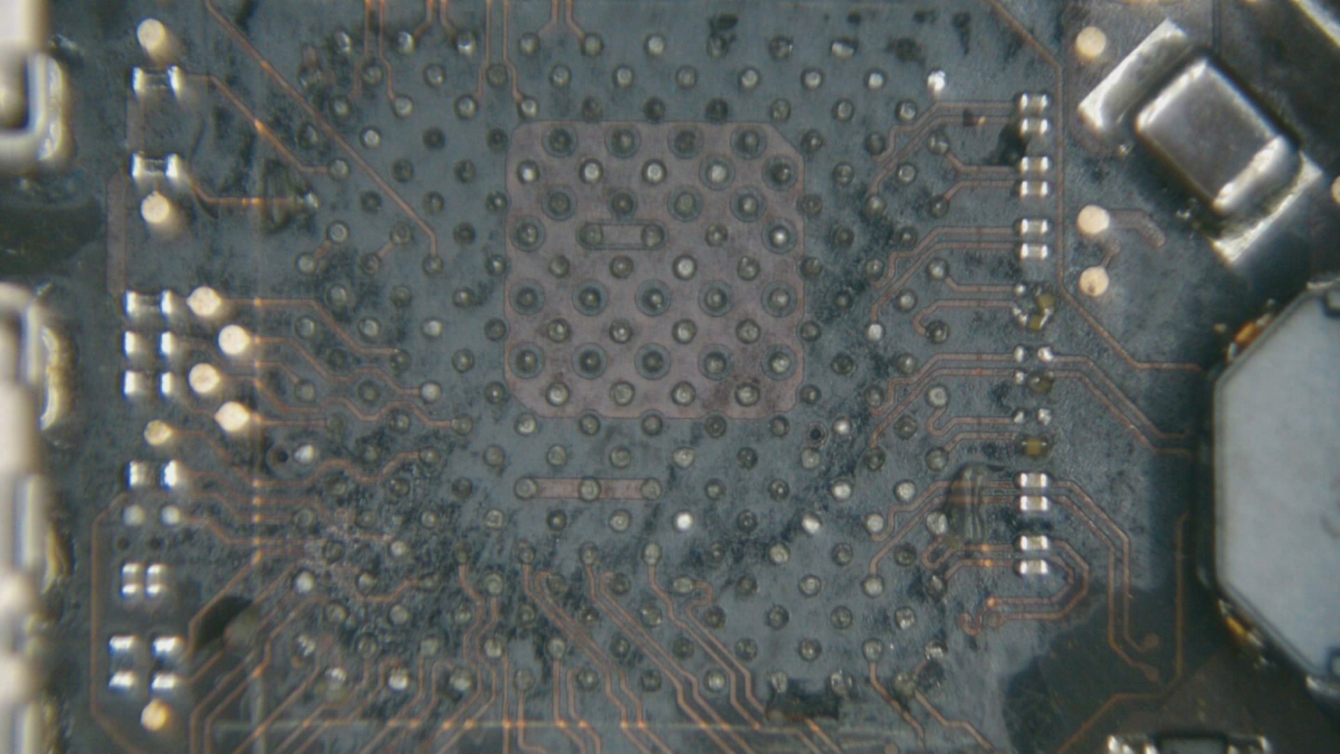
After you have successfully removed the TBT chip, you should see the line markings that we created just now.

These are the lead free solder balls that you have to remove before placing the Nevbolt-1 adapter in place.
To start wicking the lead free solder off, we personally recommend you to use the flat tip soldering iron and run the surface with leaded solder first. Apply flux to the solder balls, and begin to feed the leaded solder wire to the flat tip iron.
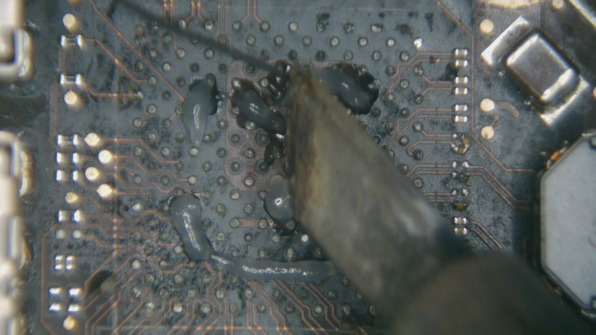
After covering all the pads with leaded solder, we will begin to use solder wick to remove the solder completely.
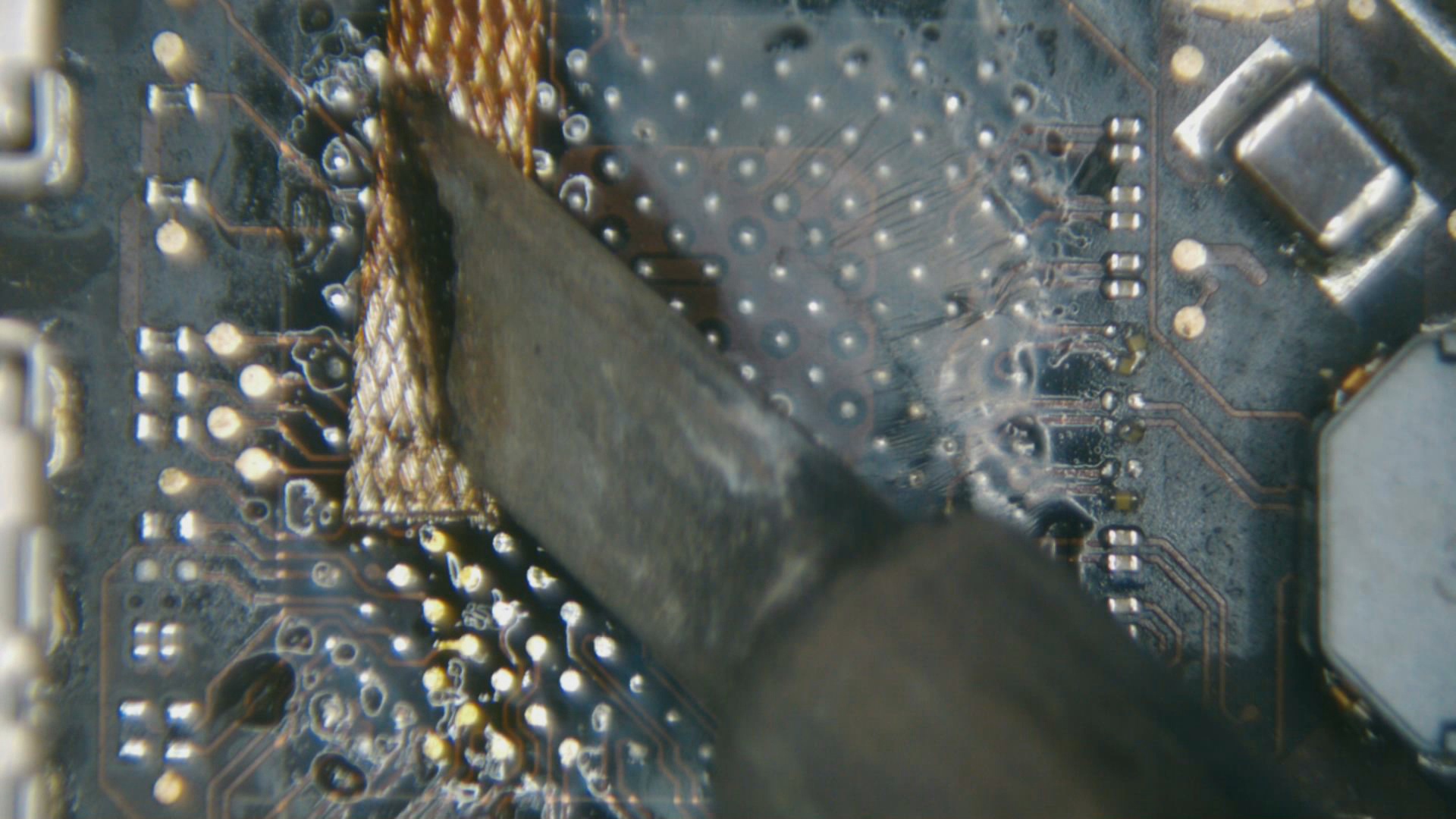
Use the Qtip(cotton bud) with 99% isopropyl alcohol to clean the mess.
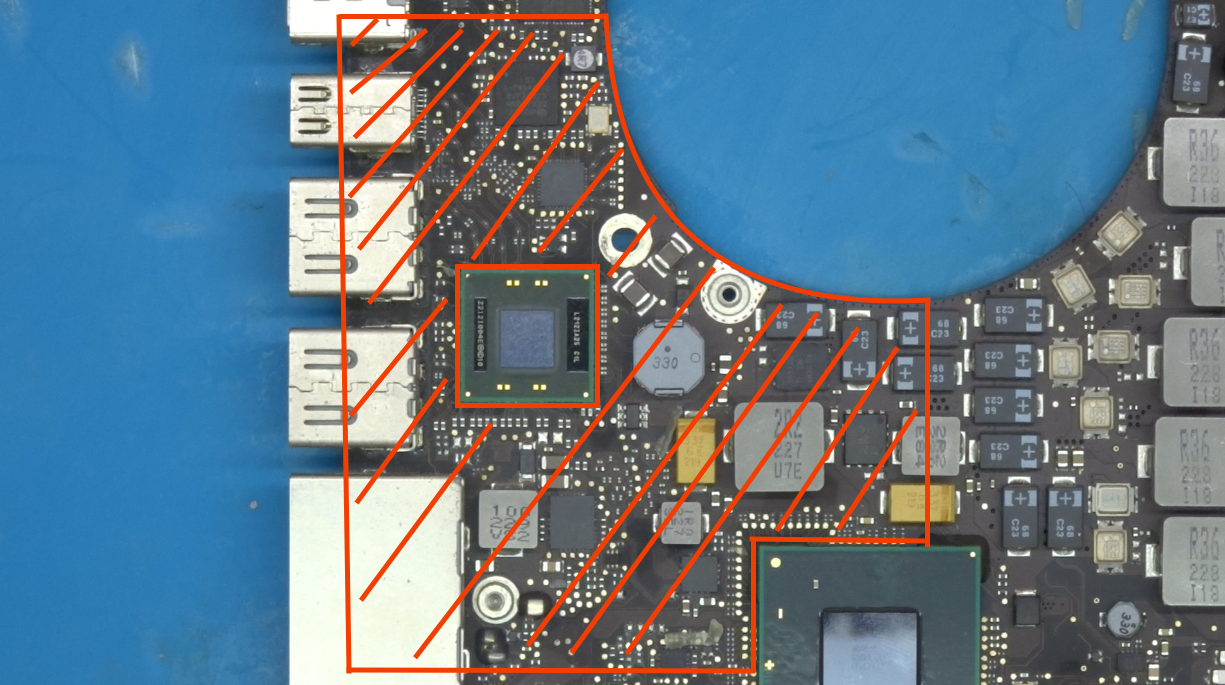
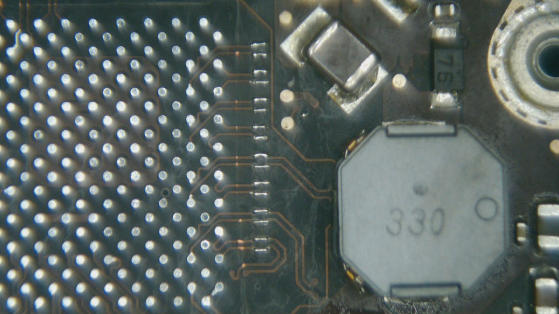
Next, we will remove all the AC coupling capacitors at the side of the Thunderbolt 1 chip. Since this is a PCIe four-lane, it has 8x differential pairs or 16x transmission lines, or we can say 16x copper traces to transmit & receive data: resulting in 16x AC coupling capacitors. These transmission lines are directly connected to the CPU.
For A1286 2012, this is the list of 16x capacitors that you need to remove, and you need to take note of each capacitor’s orientation - all of them are in horizontal position.

For A1286 2011, this is the list of 16x capacitors that you need to remove, and you need to take note of each capacitor’s orientation - all of them are also in horizontal position, but some capacitors are located at the other side of logicboard near the fan connector.

Put the nozzle back to the hot air gun and blow the hot air directly to the AC capacitors and begin to remove all of them.

Now, this is the most tedious part of the whole process, where you need to replace all the removed capacitors with 0.1mm jumper wires. You literally have to solder jumper wires to each of these 16x capacitor pads, one by one.
So we will start with the first differential pairs at the top, and it is in horizontal position. You can practically put 0201 inductor/ 33 ohm resistor to replace these capacitors but it's going to add more to the final cost.
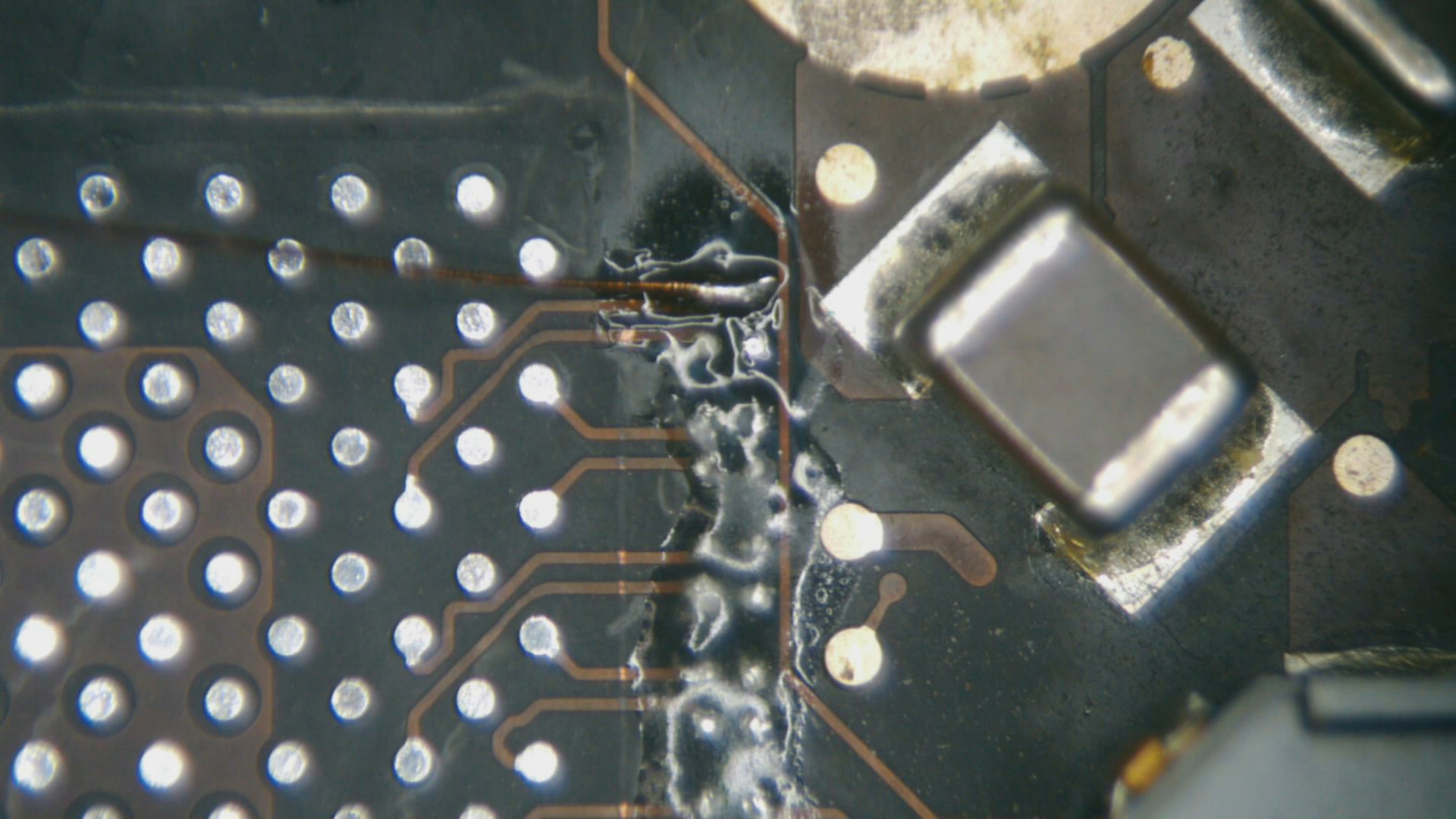
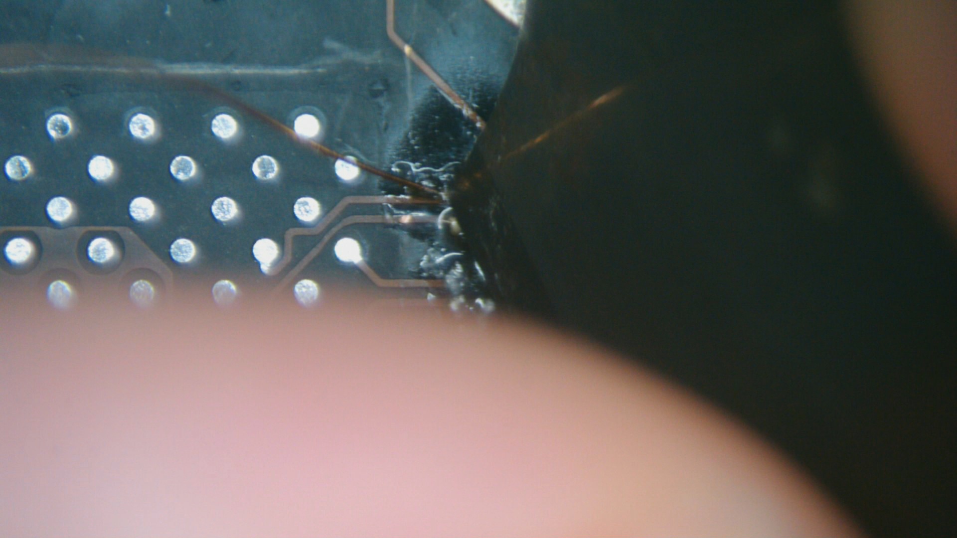
Apply flux to the pads and start to make solder bridge using 0.1mm jumper wires that should lay flat on the surface. This time we’re using a micro soldering tip to make soldering process on the 0201 solder pads much easier.
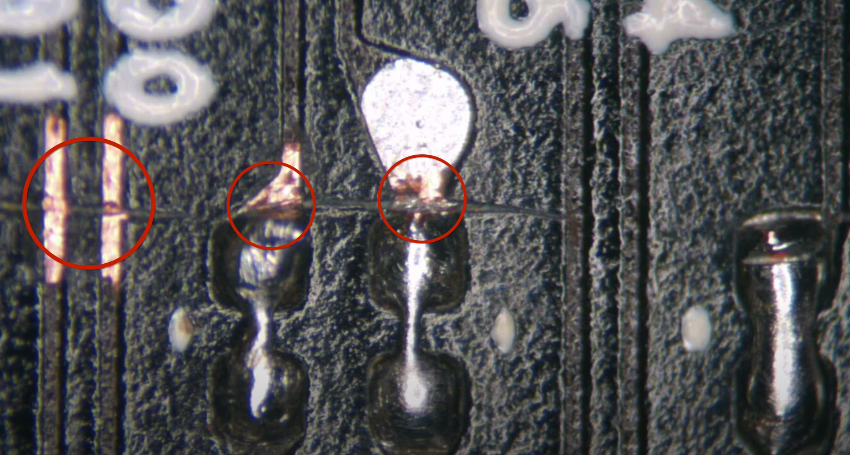
 Cut off the excess wire using a sharp blade, and make sure it is precisely cut to not have any protruding wire, that looks like this bad example as highlighted in this picture.

While your NVMe SSD might actually works without giving too much precision on these solder bridges, these protruding wires might increase the EMI and reduce the signal integrity of the high speed signals for the PCIe lanes, as a result your read&write speed will not reach the highest value as it should.
You should also be careful when using the sharp blade to not accidentally cut the copper traces like the ones in this picture, as this mistake will cause no NVMe detection at all.
 Repeat the same steps until you finish the last 8th differential pairs.
After you finish soldering all of them, you might want to reflow them a little bit with flux to let the surface tension(solder) do its job. 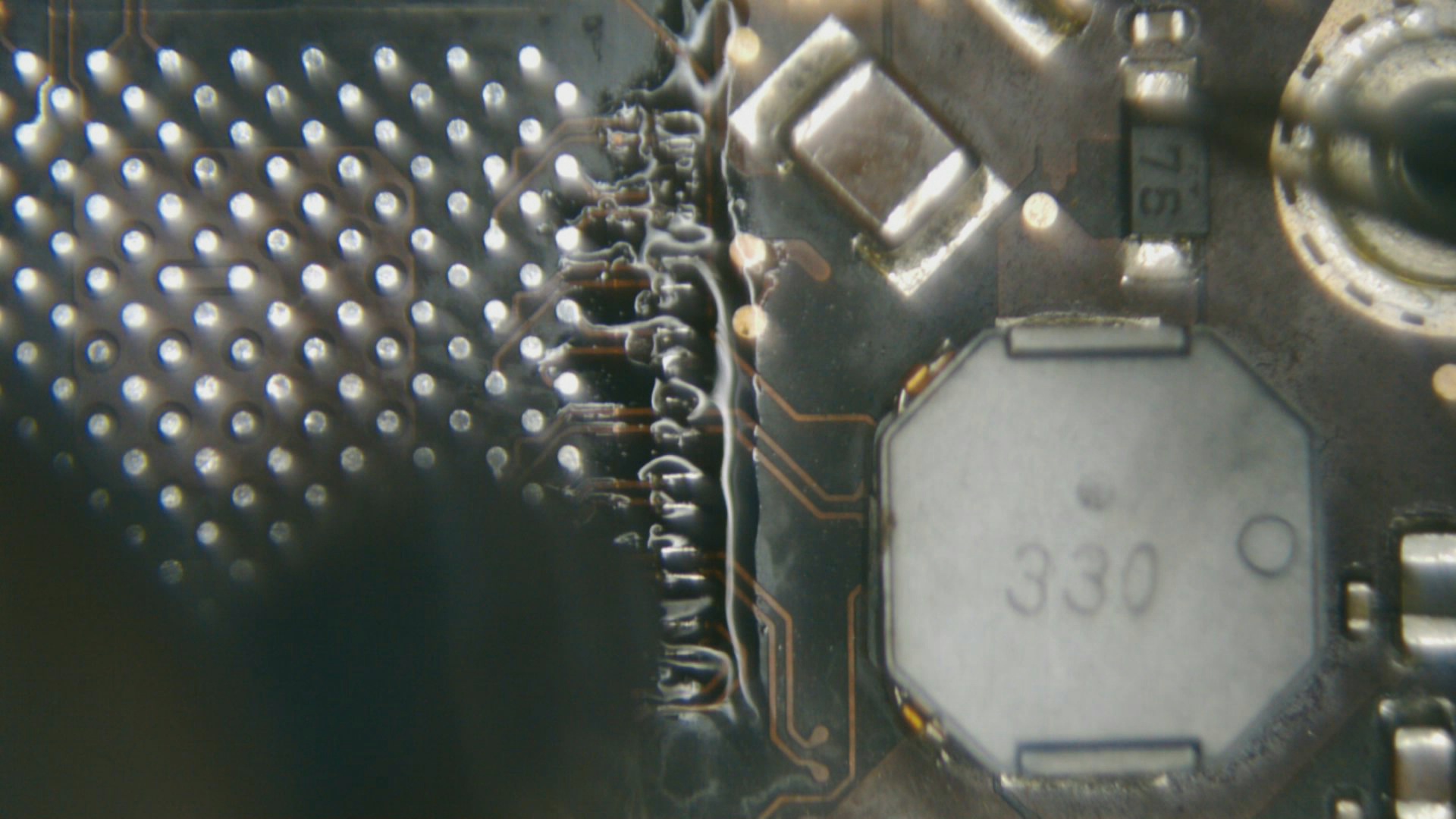

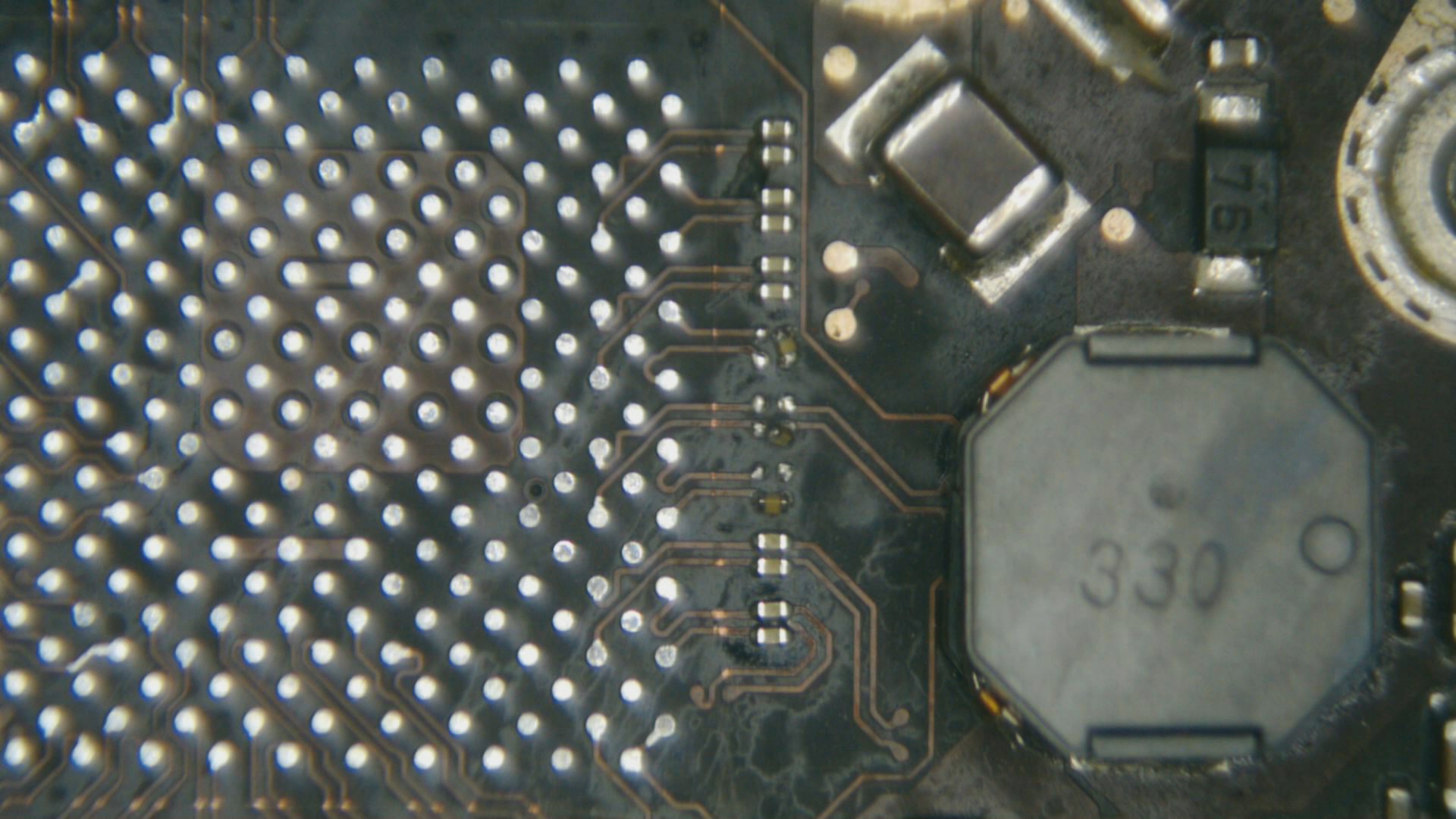
Now, if you try to take the NevBolt-2 adapter from the Upgrade Kit and try to align the NevBolt-2 adapter in place, you will find that it collides with a lot of capacitors and resistors.

These components are just Thunderbolt 1 support components(red area), so you can safely remove them now as we will not use TBT 1 anymore.
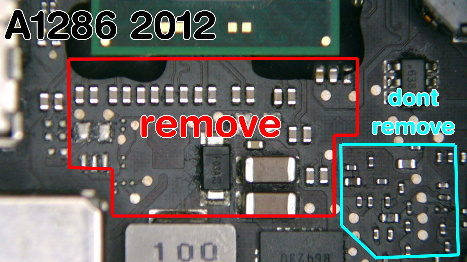
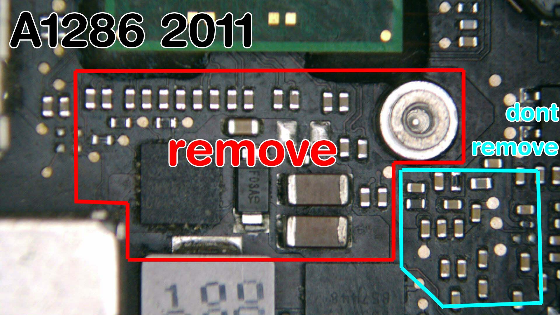
This is the components you can remove, but make sure to not remove the highlighted DP inductor(blue area). If you accidentally remove the DP inductor, you'll get blank screen. All these process are still reversible even if you removed all these components, but it will take a lot of time to restore everything.
 Now we are ready to solder the NevBolt-2 adapter to the board, so we will apply flux to the thunderbolt footprint and spread it out to all of the solder pads.
Next, locate your line markings that we have scratched earlier, and use them as your placing guide. We will represent these line markings as a red square, so now you need to place the NevBolt-2 and try to adjust and align the square part of the NevBolt-2 precisely into the red square.
Take off your hot air nozzle again and perform the same preheating steps to the local area of the MLB. After 40 seconds or so, you can target the heat directly to the center of the NevBolt-2, but this time it won’t take too much heat to reach liquidus(185C) because the NevBolt-2 balls are actually leaded solder balls.
Let it cool for a few minutes, and after the heat is gone, you can slowly try to nudge it to determine whether it's properly soldered or not.

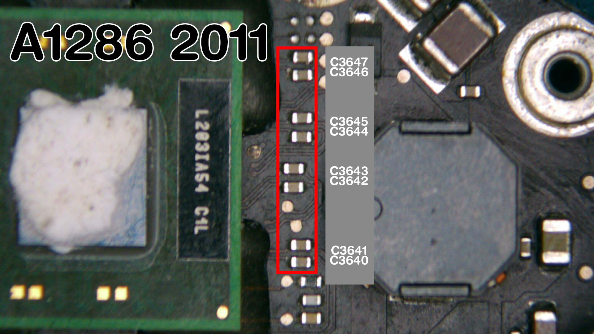
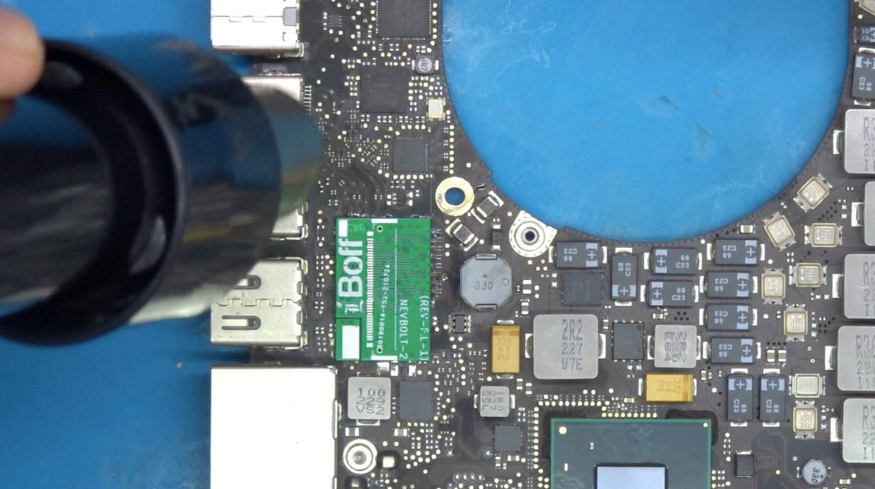
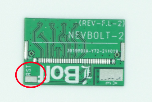
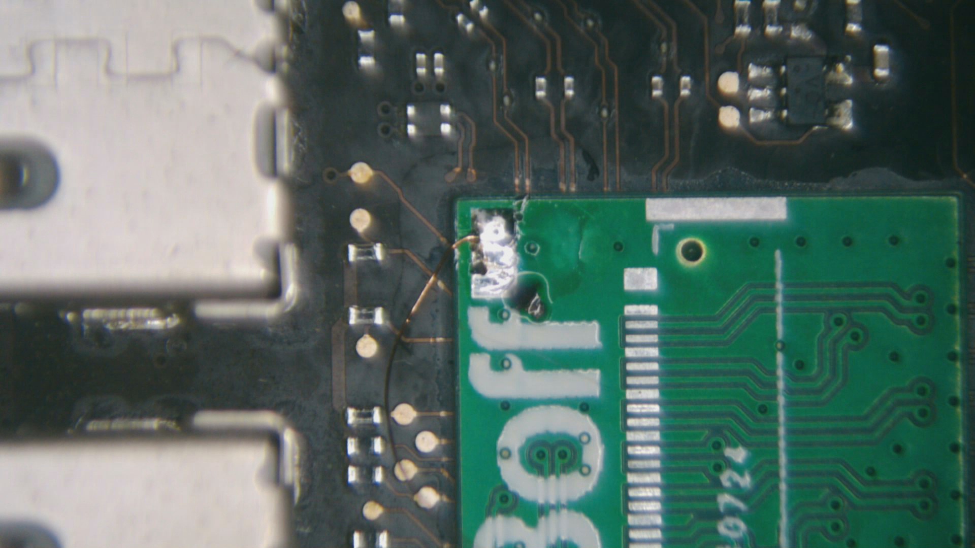
The next step is you need to find the RST pad on the NevBolt-2 adapter,
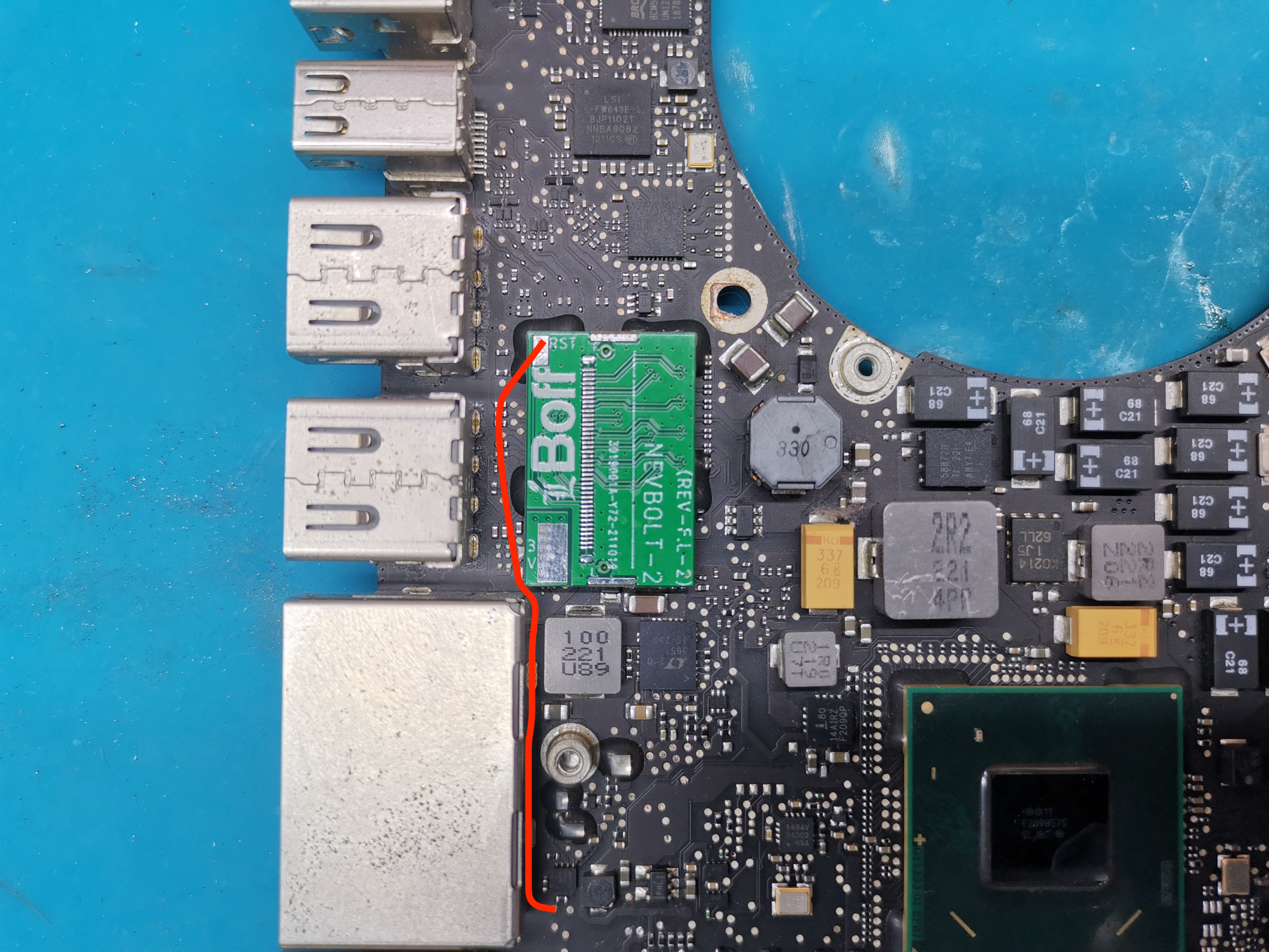
 then you need to connect the “PLT_RST_BUF_L” signal to this pad using 0.1mm jumper wires. The closest location that you can pull the signal is from the R3803.
 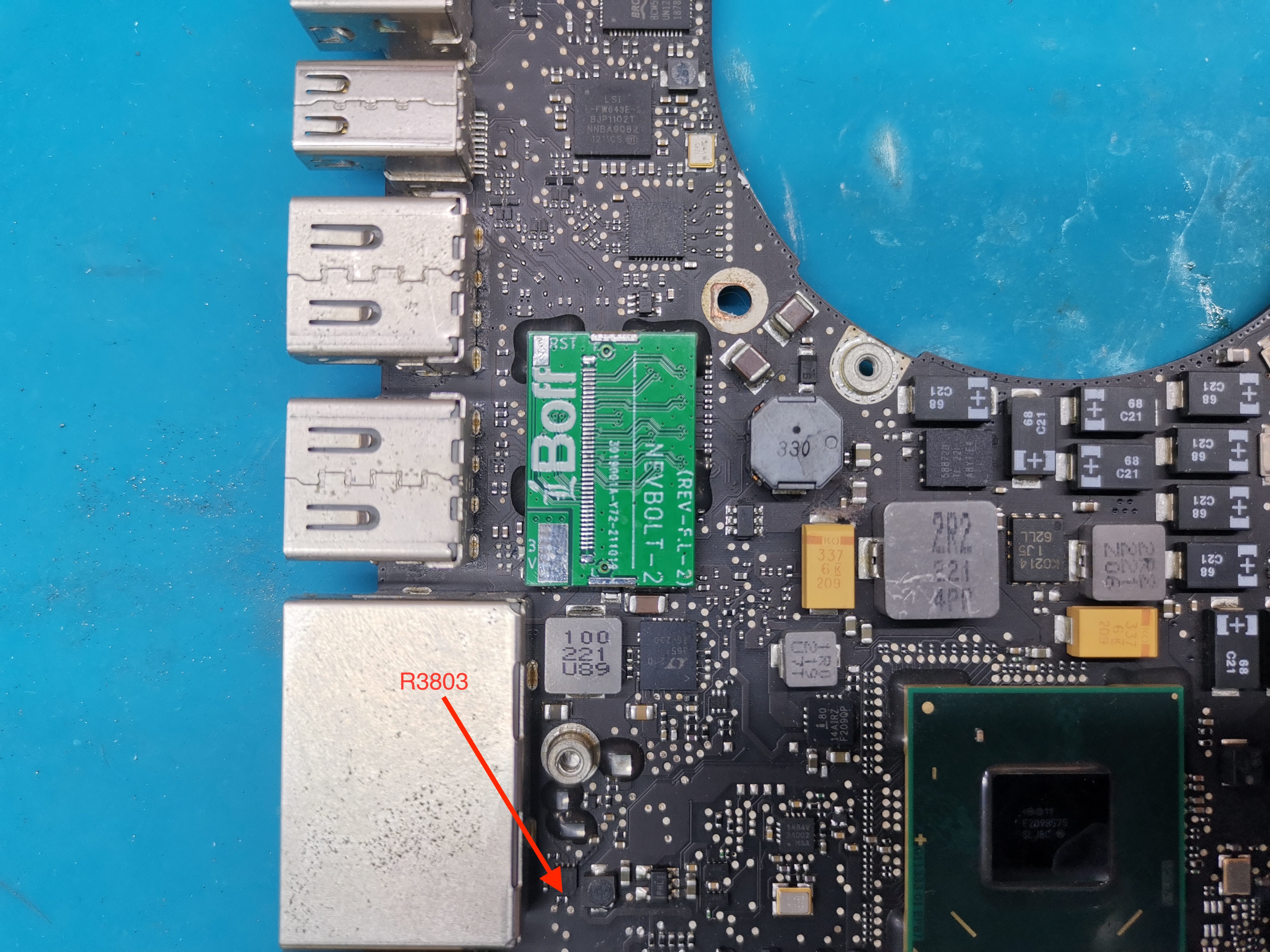 Solder the wire to pin no 2, and connect the other end of the wire to the RST pad and cut the excess wire.
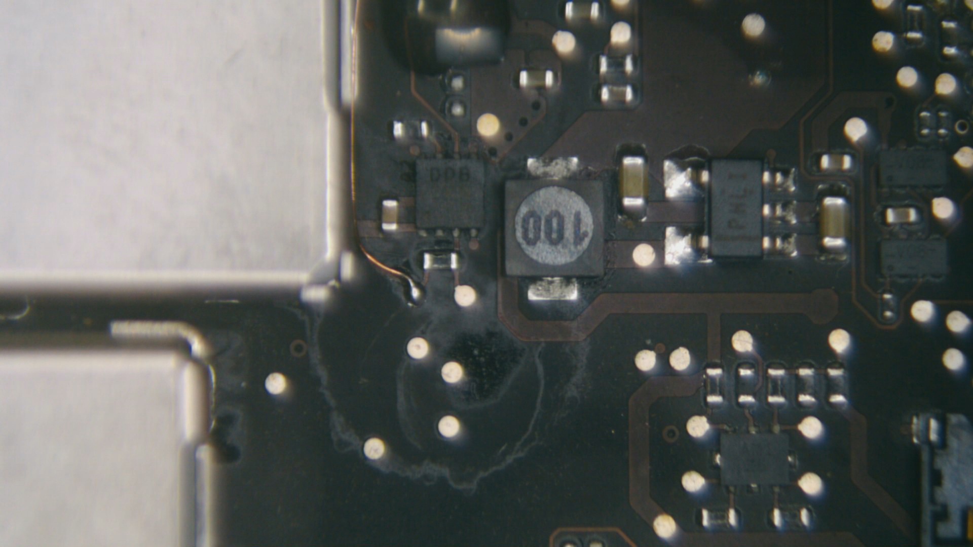
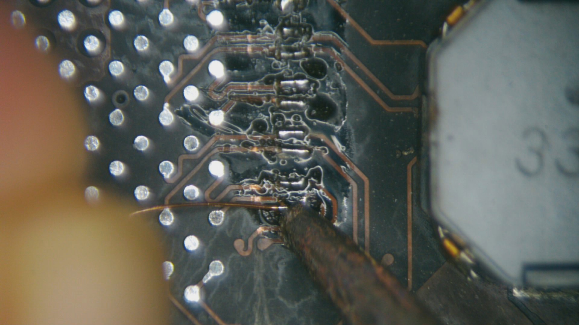
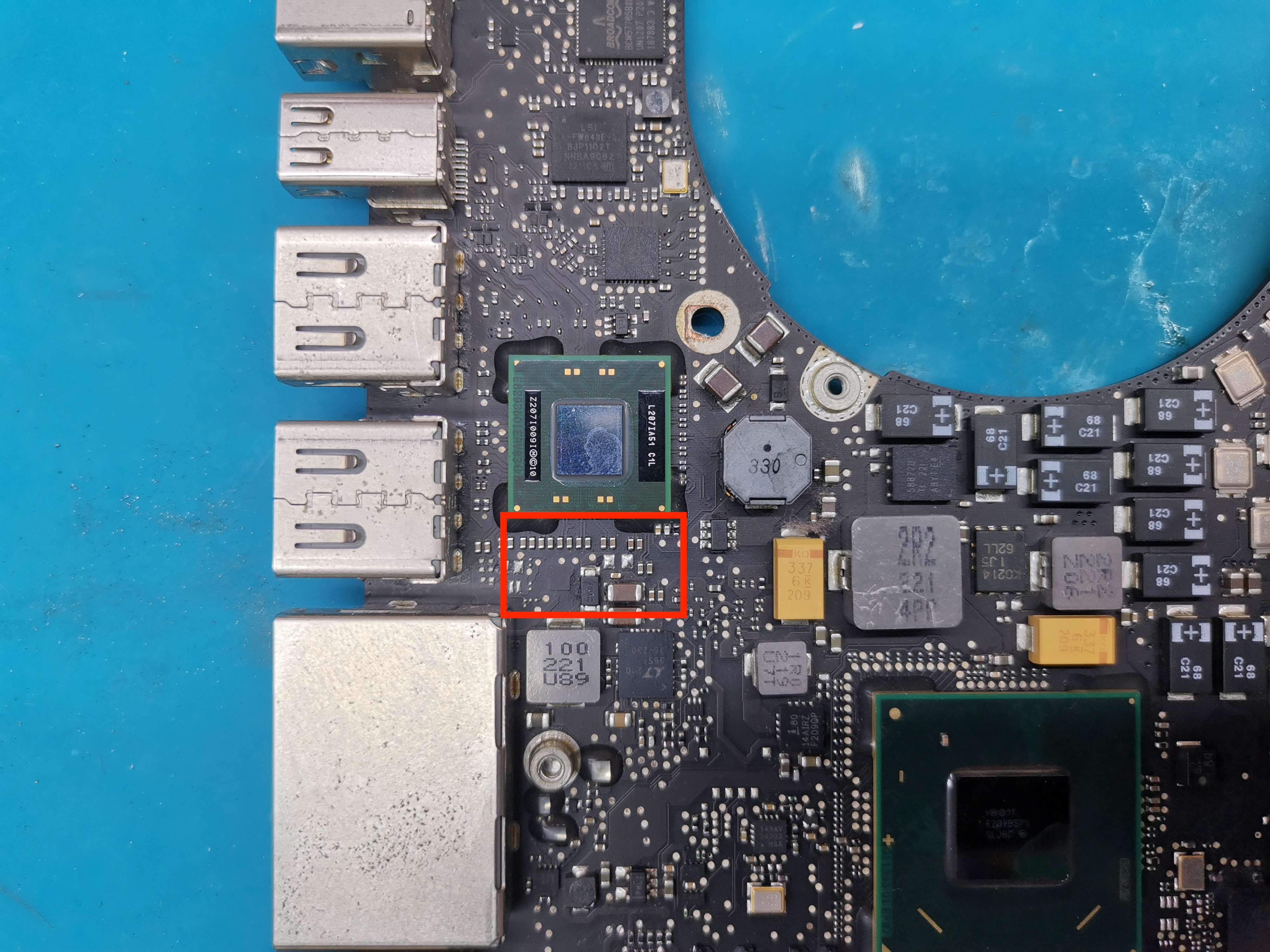
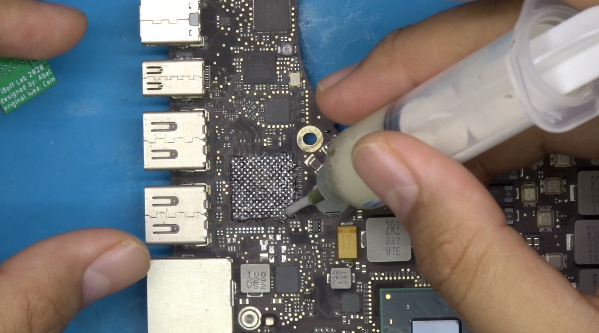
Next, find the U3810. You need to remove this Load Switch and create a solder bridge connecting both PP3V3_S0 & PP3V3_T29.
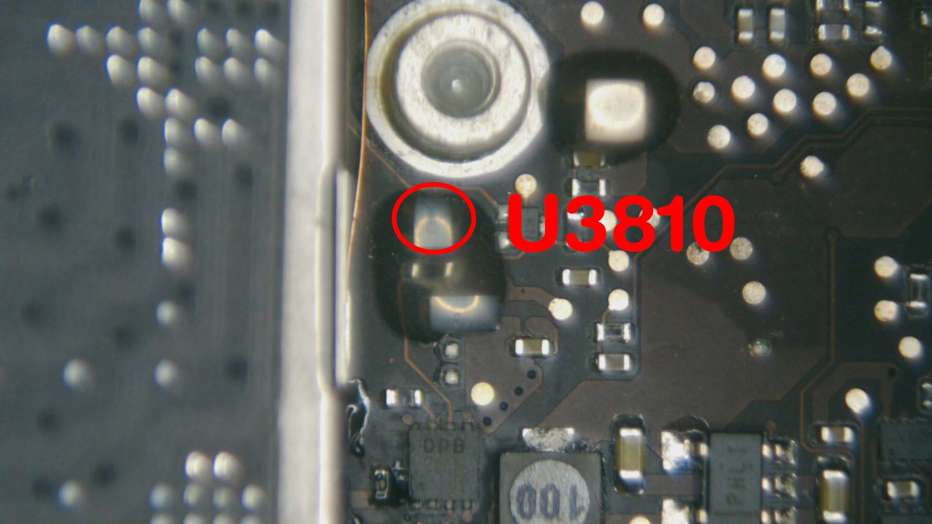
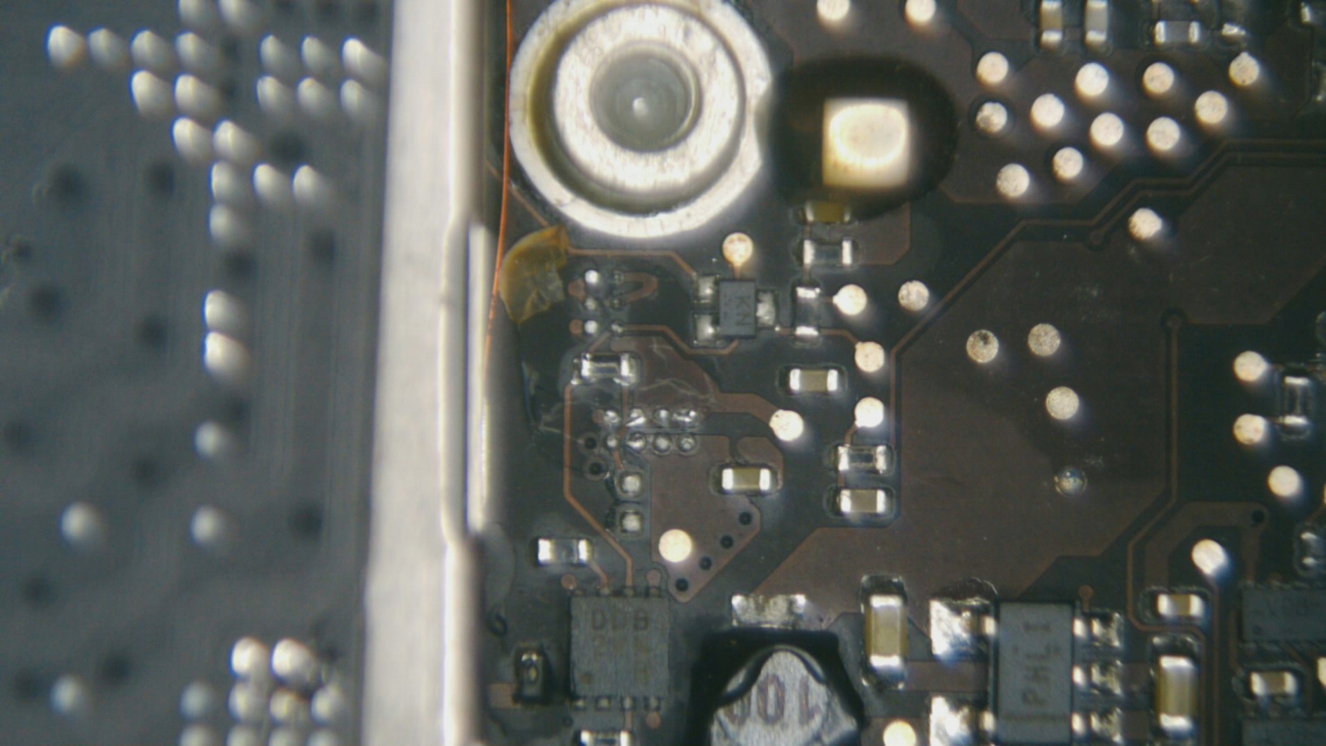
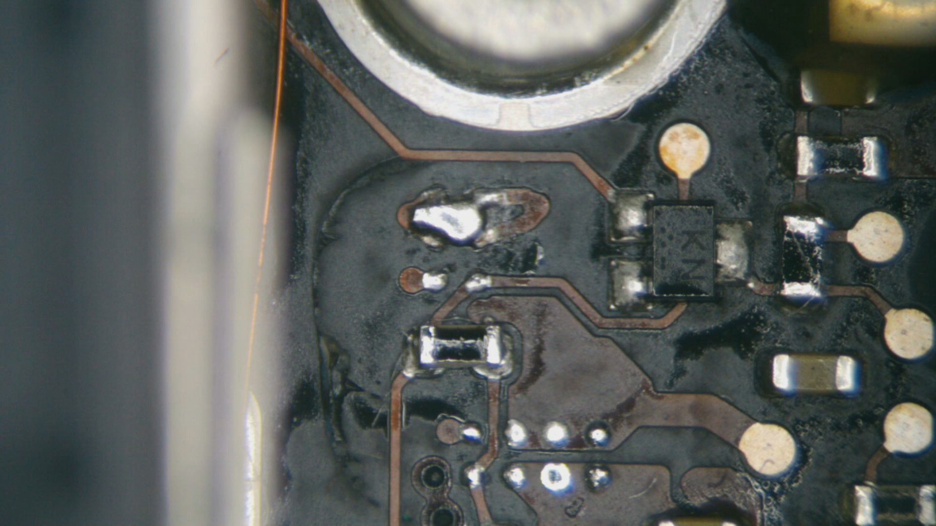
The reason why we have to do this is because the Load Switch is only able to deliver a maximum current of 2 Amps @ 3.3 Volt, while the aftermarket NVMe like the Samsung 970 EVO requires 3.3 Amps @ 3.3 Volt to operate properly. Insufficient power delivery to the NVMe SSD will cause unstable read/write performance, and the Load Switch U3810 might blown up for drawing current more than 2 Amps. This also means that if you want to reduce battery consumption, you need to buy a newer generation of NVMe SSD that has a low power rating, say, power rating of 1 [email protected] Volt. So we need to remove the underfill covering the Load switch, and blow the hot air gun directly to remove the switch. Use the 0.1mm jumper wires to create a solder bridge between PP3V3_S0 & PP3V3_T29.
Now you can take the I-PEX female connector supplied from the Upgrade Kit, and you can solder it to the NevBolt-1 just like you solder the LVDS port for the LCD.
Before placing the IPEX connector in place, you need to apply flux to pads, and align the connector to the footprint.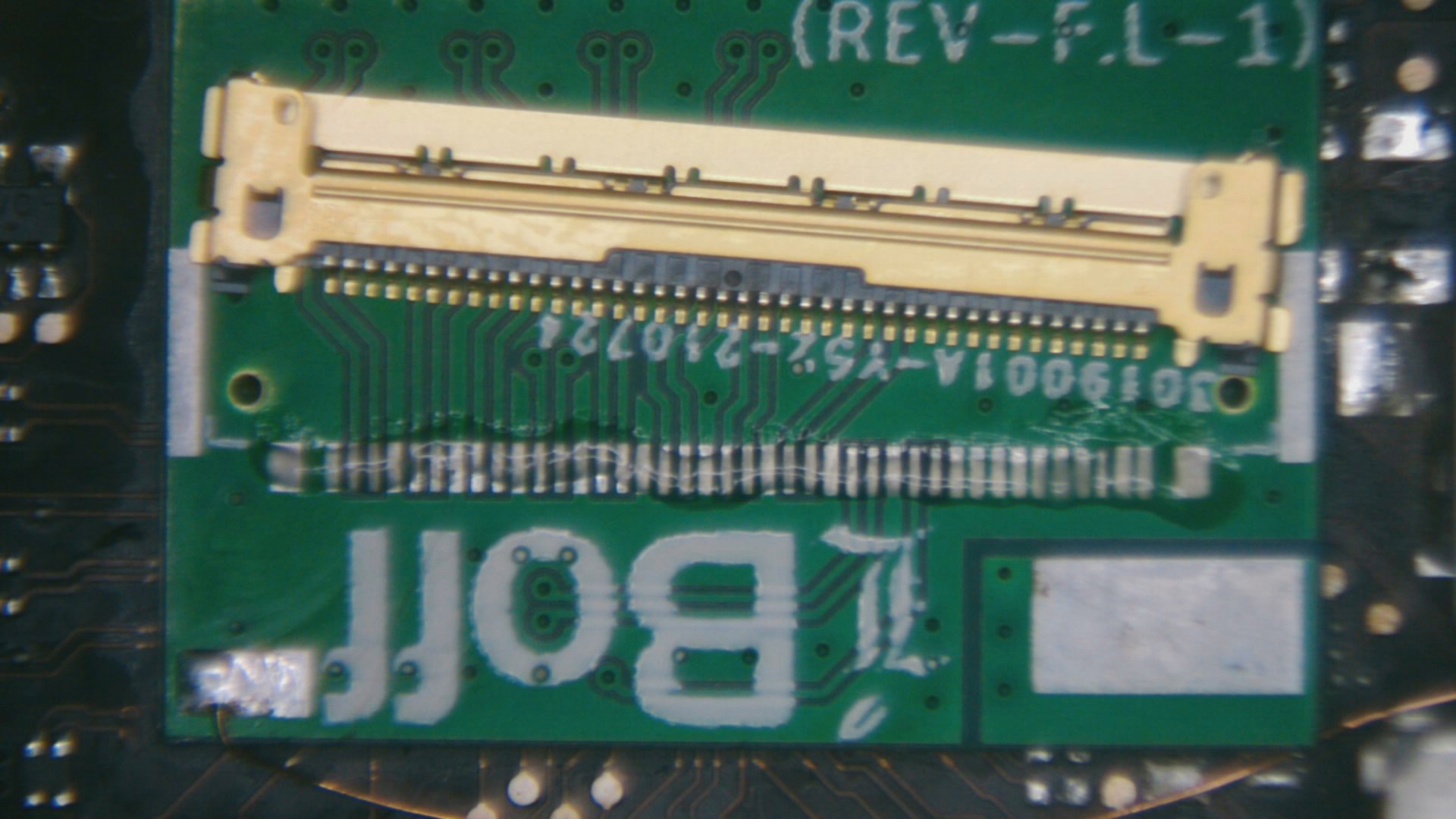
Put the tweezers on notches at the topside of the IPEX connector to help you hold it in place. 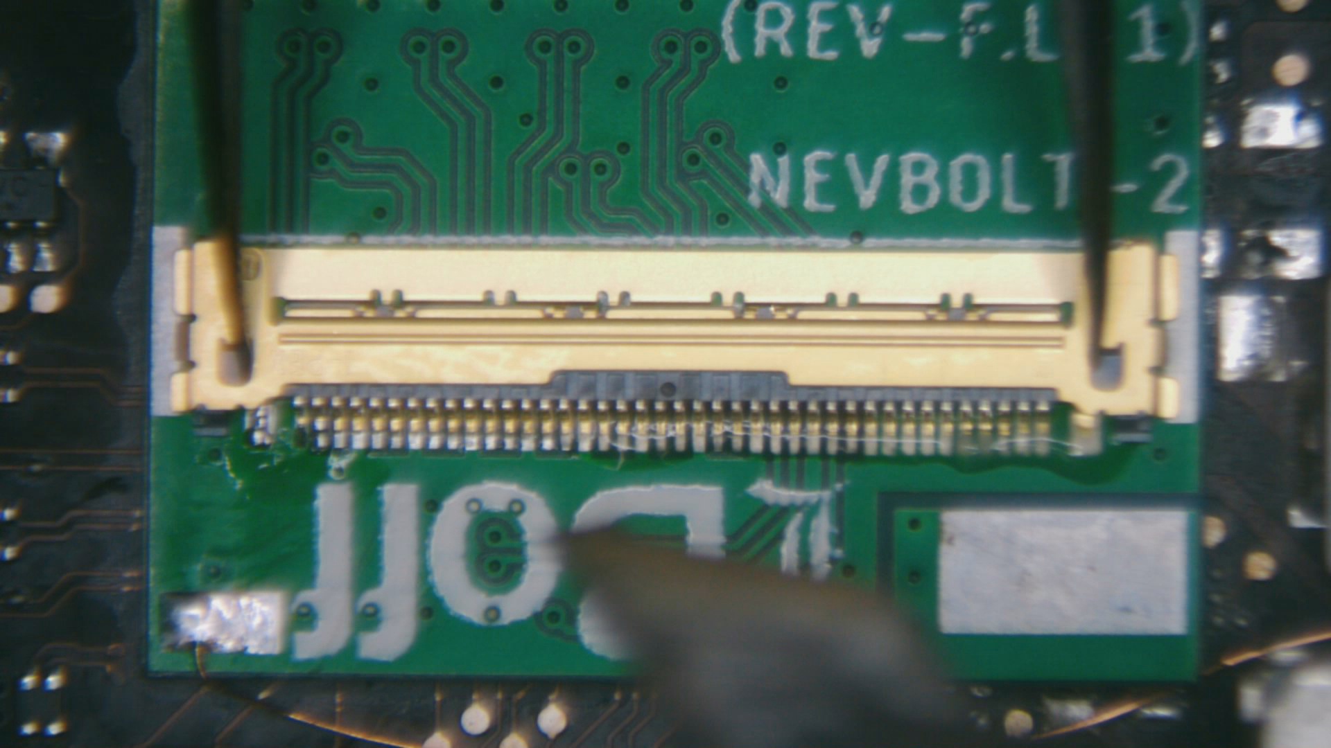
By using flat tip soldering iron, you can see that we place a solder blob at the tip of the iron, and begin tapping on the first and the center pins of the connector to help it stay in place.
 So now you can release the tweezers and proceed to solder the rest of the pins, and you can add more flux where necessary. Lastly, you need to solder both of the left and right side of the housing for better grounding and stronger support.
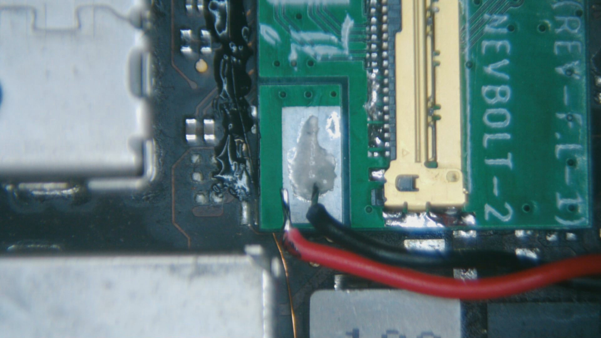
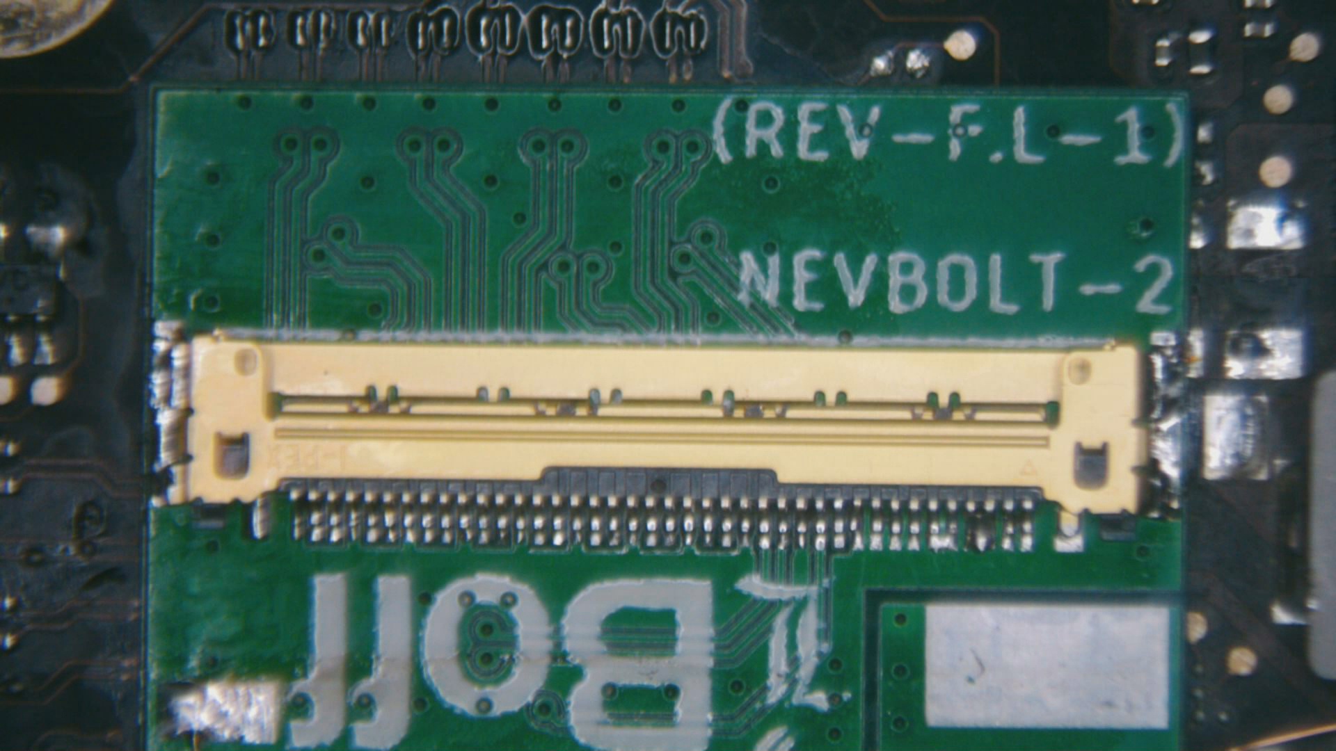 If you want to clean the MLB with the ultrasonic cleaner, you can do it now. Next, take the 3.3V power wires from the Upgrade Kit, and before soldering it to the NevBolt, you can wind them up to make it look neat. Now we need to solder both of the red&black wires to the 3.3volt pad, eventhough we know that usually Black is for GND, and the Red is for Power.
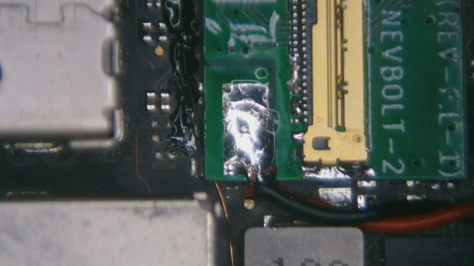
Before we finalize the soldering process, it's a good idea to clean the area a little bit with Qtip and isopropyl alcohol, and you can use the UV solder mask to cover the exposed PLT_RST_L wire. This is also the right time to reapply the thermal paste to the CPU if necessary, and you can begin to reassemble the whole as usual. *to be updated soon