iPad Pro with OLED may be more expensive because of dry etching
 Andrew Orr
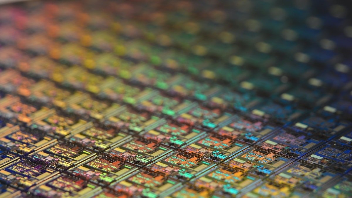
Silicon wafer. Photo by Laura Ockel on Unsplash
Apple is rumored to bring OLED displays to the iPad Pro by 2024, manufactured using a technique called dry etching to ensure the screens remain as thin as possible. Unfortunately, this will also likely make these iPads more expensive. Here's why.
If the report about OLED iPad Pro models is taken at face value it could mean that Samsung will be a manufacturer responsible for producing the displays. The company did supply OLED panels for the iPhone 12 and iPhone 13. However, the report provided no sources other than saying "Apple confirms."
Dry etching is not new. The U.S. Patent Office granted a patent to Samsung in 2004 for a dry etching apparatus.
The patent describes a vacuum chamber where the etching takes place, a "chuck" that holds the substrate, and another part called a "baffle plate" that encloses the chuck and discharges the products used for etching. Whether Samsung still uses this particular apparatus is unknown, but vacuum chambers are necessary during the dry etching process due to the plasma.
Types of etching
Samsung describes wet etching as cheap, fast, and simple. Dry etching wafers is more precise and less prone to contamination but is expensive and complex. Thus, if Samsung uses this method for producing OLED screens, it may increase the iPad's price.
Etching is a process that removes unwanted material from a wafer, which is also known as a "slice" or "substrate." Wafers are made of semiconducting material such as crystalline silicon and are used in the fabrication of integrated circuits and solar cells.
Dry etching uses gaseous chemicals or plasmas to remove materials from a wafer, while wet etching uses liquid chemicals, such as solvents and acids. Both methods have benefits and downsides.
Wet etching
A wafer is submerged in certain chemicals during wet etching, depending on its material. For example, buffered hydrofluoric acid is commonly used with silicon wafers.
Like any manufacturing process, there are waste streams. Hydroflouric acid and the materials dissolved in the run-off from manufacturing must be appropriately disposed of to prevent water contamination. In addition, the solvent may remove more material from the wafer than is ideal.
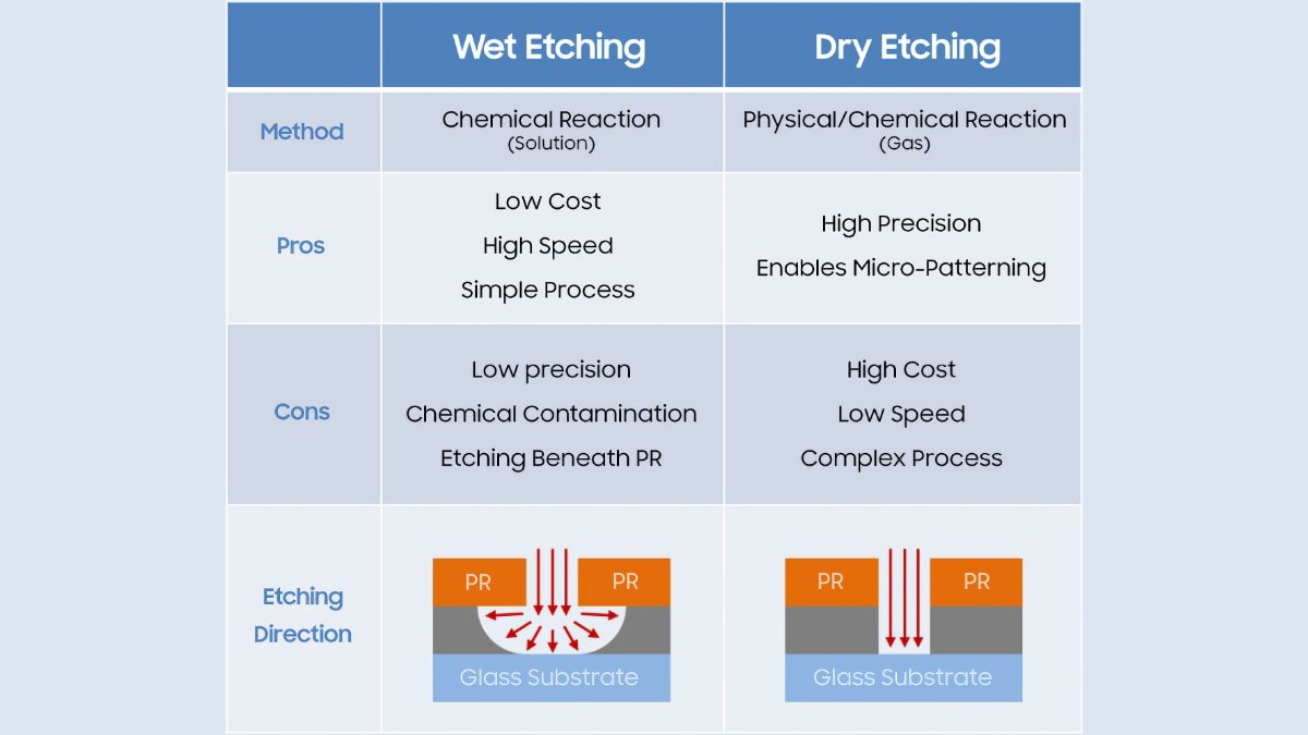
In Samsung's chart, "Etching beneath PR" found under wet etching refers to the photoresist, a material sensitive to light that changes its properties during photo lithography. The result is intricate circuits on the thin film transistor (TFT) that the display itself is applied to.
Samsung and other manufacturers use wet etching for Apple's existing OLED supply for the iPhone.
Dry etching
A manufacturing alternative is dry etching, which is more precise and can remove substrate materials in different shapes than wet etching.
Dry etching is commonly used in very large scale integration (VLSI) processes that produce integrated circuits. There are a few methods in dry etching, such as isotropic radial etching, reactive ion etching, sputter etching, and ion milling. The intricacies of each are beyond the scope of this article, and differ based on how the process removes semiconductor materials from the wafer.
All variants of dry etching processes use plasma, which is why dry etching is often referred to as plasma etching. Ion milling and sputter etching use a beam of ions to eject or vaporize material physically.
Samsung's article describes plasma etching, where gas is injected into the vacuum chamber containing the wafers and energized to become plasma. Then, ions that gain high kinetic energy are beamed onto the wafer to remove semiconductor material.

In both types of etching, the photoresist acts as a protective film for the circuit pattern during the etching process. After etching, only layers coated with PR to be used as the circuit are left on the glass substrate. All other materials are removed.
Manufacturing
While dry etching isn't strictly new, it's not used in much at present.
In 2021, Gerald Yin, chairman of Chinese semiconductor equipment company AMEC, said the company's plasma etching equipment was being used in a customer's 5nm chip production.
AMEC didn't reveal the customer, but at the time the only ones capable of 5nm mass production were TSMC and Samsung, two companies that have served as manufacturers for Apple. In June 2022, TSMC posted a job listing for a "Dry Etching Process Engineering Manager" at its 5nm fab in Arizona.
Samsung's patent says that a dry etching apparatus using plasma is suitable for fabricating circuits with a width of 0.15 micrometers or less. The company concludes that dry etching is the preferred method for high-resolution displays.
The Apple supply chain will likely keep using the wet etching process for iPhone and Apple Watch. It's a cheaper solution that produces a display still lighter than an LED screen with a higher quality, at a relatively low price.
Dry etching is better products with large OLED displays. The process costs more but its precision is beneficial for these large displays where weight is a factor.


 Malcolm Owen
 William Gallagher and Mike Wuerthele
 Christine McKee
 William Gallagher

 Marko Zivkovic